The article focuses on wafer shape control in semiconductor manufacturing, specifically in the context of memory device Z-height scaling. The main challenges discussed include global and local stress in wafers, which can lead to warping, misalignment, and overlay issues during semiconductor processing. The study introduces a novel technique involving thin film deposition combined with ion implantation to manage these stresses and achieve improved wafer flatness.
Challenges in Wafer Shape Control:
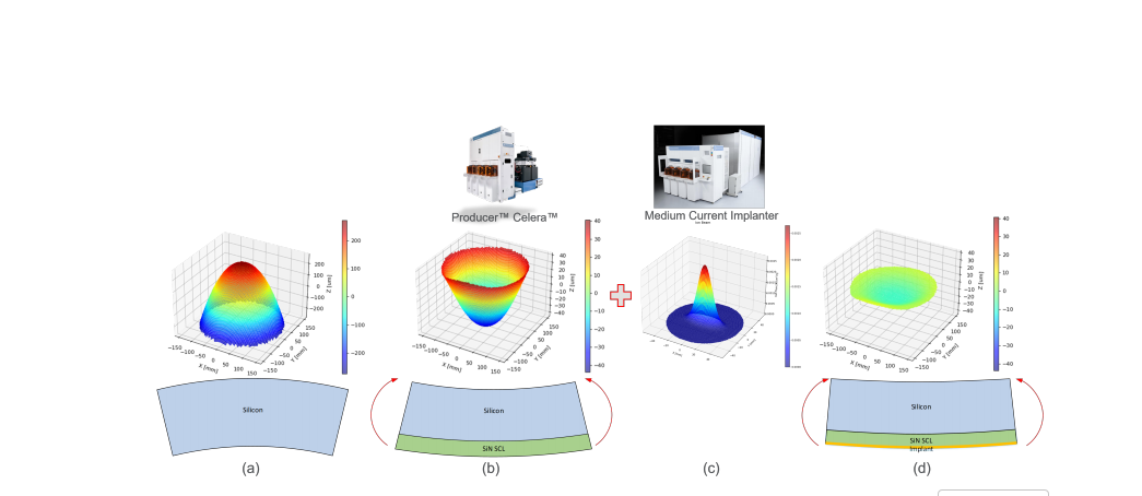
The article highlights how global parabolic warps and local patterning-induced stresses lead to saddle-shaped wafers. These deformations can affect the wafer's chuckability (ability to be held in place during processing) and lead to overlay issues, ultimately reducing yield and device performance.
Proposed Solution: Wafer Stress Management (WSM):
The authors propose a co-optimization method using dielectric film deposition for stress compensation and ion implantation to modulate the wafer's stress locally.
By carefully adjusting film properties (stress and thickness) and implant parameters (species, energy, dose), the method can correct both anisotropic global warping (such as saddle shapes) and local warping.
Application in 3D NAND and HBM Devices:
The 3D NAND memory devices and High Bandwidth Memory (HBM) integration are used as examples where this stress control technique is crucial. The saddle shape induced by high-aspect-ratio structures in NAND is corrected with this approach, which ensures better alignment and processing efficiency.
Wafer bonding, particularly in die-to-wafer (D2W) and wafer-to-wafer (W2W) processes, benefits from this technology, which enhances the bonding strength, alignment, and reliability of stacked dies.
Optimization of Stress Control:
The paper describes the use of a customized dose map to correct the wafer's shape by adjusting the stress compensation layer (SCL) and ion implantation. This technique has been validated in high-volume manufacturing (HVM) environments and offers an efficient solution to address saddle shapes and local stress variations.
Results and Effectiveness:
The technique has shown impressive results, such as reducing saddle skew by over 90%, significantly improving chuckability and overlay precision. For example, in HBM die bonding, the method reduced out-of-spec dies from 63.4% to 7.6% after applying the WSM approach.
Future Directions:
The study also extends to thinned wafers and die-level corrections, addressing the deformation challenges during die singulation and wafer thinning. This method improves die yield and wafer-level Z-height control, ensuring the quality of advanced packaging solutions.
The paper proposes an innovative and effective approach to wafer shape control, combining thin film deposition and ion implantation to manage stress variations. This method resolves the challenges of global and local wafer warping, ensuring better chuckability, overlay accuracy, and yield in advanced semiconductor manufacturing, particularly for 3D NAND and HBM devices. This process plays a critical role in scaling up high-performance memory devices and enabling more efficient 3D integration in AI and high-bandwidth applications.
OMeda (Shanghai Omedasemi Co.,Ltd) was founded in 2021 by 3 doctors with more than 10 years of experience in nanpfabrication. It currently has 15 employees and has rich experience in nanofabrication (coating, lithography, etching, two-photon printing, bonding) and other processes. We support nanofabrication of 4/6/8-inch wafers.