The article provides an in-depth review of co-packaged optics (CPO) and 3D optoelectronic integration, focusing on innovations, challenges, and future trends in high-speed data communications. The study highlights the key advancements in these areas that aim to meet the rising demands for bandwidth, energy efficiency, and low latency in data centers, artificial intelligence (AI), and high-performance computing (HPC).
Co-Packaged Optics (CPO):
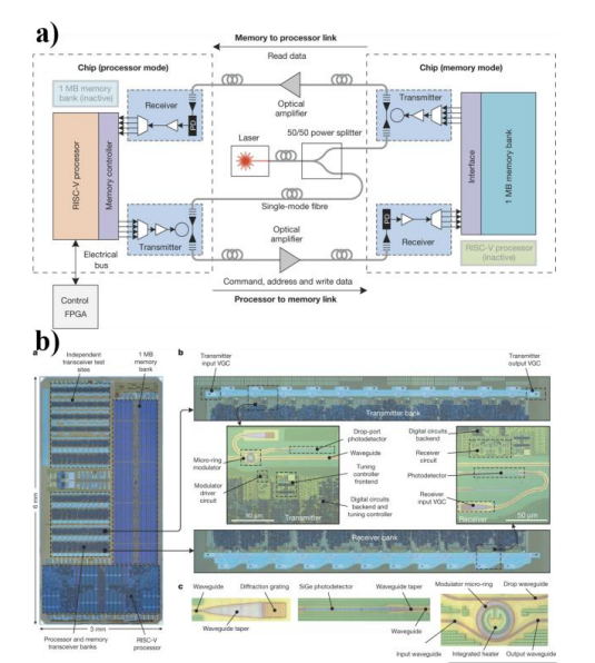
CPO represents a transformative leap in optical communications by embedding optical transceivers alongside electronic circuits in the same package, significantly improving energy efficiency and bandwidth density.
Traditional pluggable optics are being replaced by on-board optics (OBO) and CPO, which shorten electrical links, reduce energy per bit, and enhance signal integrity.
The integration of optical transceivers directly with switch ASICs reduces the power consumption from 15-20 pJ/bit (in pluggable optics) to 5-10 pJ/bit in CPO systems.
Packaging Methods and Integration:
2.5D and 3D integration techniques are being employed to improve bandwidth density and reduce signal degradation. These methods use interposers or bridges with through-silicon vias (TSVs) for efficient communication between photonic and electronic components.
3D stacking enables extremely high-density integration by placing electronic and photonic devices directly on top of each other, but it introduces challenges in thermal management and fabrication complexity.
Technologies and Components:
Advances in silicon photonics, VCSELs (Vertical-Cavity Surface-Emitting Lasers), and heterogeneous integration are key enablers for CPO. Silicon photonics excels in long-reach applications and WDM (wavelength-division multiplexing) scalability, while VCSEL-based solutions offer excellent energy efficiency for short-reach connections.
Power dissipation and thermal management are critical challenges in CPO systems, particularly as high-power ASICs and photonics are integrated within the same package.
Challenges in Manufacturing:
Alignment tolerances, coupling losses, and thermal management remain significant obstacles to the wide adoption of CPO. Advanced microfluidic cooling, thermal interface materials (TIMs), and new packaging solutions are being explored to address these issues.
The standardization of process design kits (PDKs) and packaging interfaces is vital for improving manufacturing yields and enabling interoperability across vendors.
Applications:
CPO is already being explored in a range of applications, from hyperscale data centers and AI clusters to quantum networks, 5G/6G communications, and automotive LiDAR systems.
The integration of optical sensors and quantum photonics for distributed quantum computing and secure communication is a growing area of interest.
Future Research Directions:
The article discusses future trends, such as the integration of LiNbO3 (Lithium Niobate) modulators, III-V materials for lasers, and the use of AI-driven photonic accelerators for applications in optical computing and AI-based networks.
The convergence of monolithic integration and chiplet-based approaches could be the future of scalable photonic-electronic integration.
Co-packaged optics and 3D optoelectronics are set to revolutionize the way high-speed data is transmitted in data centers, AI systems, and beyond. While there are still challenges in thermal management, precision manufacturing, and cost, these innovations promise substantial improvements in energy efficiency, bandwidth density, and latency. As these technologies evolve, they will play a crucial role in shaping the future of high-performance computing and networking systems.
OMeda (Shanghai Omedasemi Co.,Ltd) was founded in 2021 by 3 doctors with more than 10 years of experience in nanpfabrication. It currently has 15 employees and has rich experience in nanofabrication (coating, lithography, etching, two-photon printing, bonding) and other processes. We support nanofabrication of 4/6/8-inch wafers.