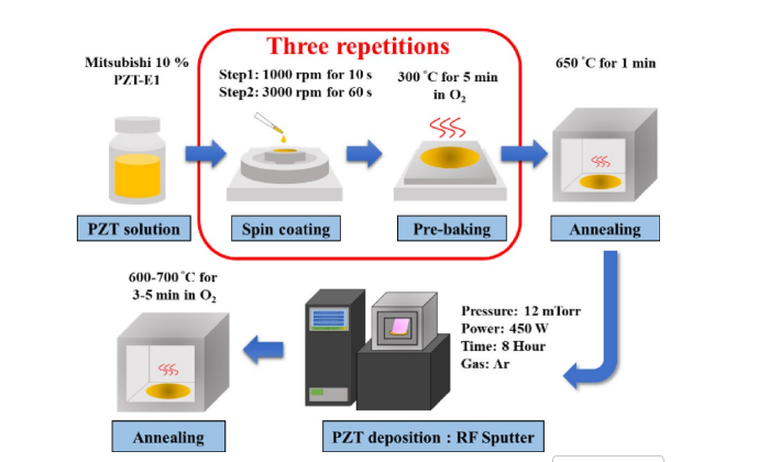
This study introduces a cost-effective and reliable method for fabricating PZT (Lead Zirconate Titanate) thin films used in piezoelectric micromachined ultrasonic transducers (pMUTs). The process employs a commercial sol-gel solution as a seed layer, followed by RF sputtering to deposit the PZT thin film. This approach addresses issues related to thermal expansion mismatches and cracking, which are common in conventional PZT fabrication methods.
The research demonstrated that the PZT thin film fabricated using this method exhibited high remnant polarization (Pr) and a coercive field (Ec), making it suitable for high-performance applications. Specifically, the film achieved a maximum Pr of 113.35 µC/cm² and Ec of 211.6 kV/cm, which were among the best reported values for air-coupled PZT-based pMUTs.
Furthermore, the study presents the design and fabrication of pMUTs and their arrays, which operate efficiently in mid-air ultrasonic applications such as haptic feedback and acoustic levitation. The fabricated pMUT arrays demonstrated significant acoustic pressure outputs, with the highest output reaching 87.4 Pa at a 3 cm distance from the array. The study also highlighted the superior transmission efficiency of these pMUTs compared to other air-coupled PZT-based devices, making them promising for advanced sensing technologies and human-machine interfaces.
In conclusion, this work provides an innovative and scalable solution for producing high-performance PZT thin films and pMUTs, with applications ranging from fingerprint recognition to ultrasonic haptic feedback and range detection, all while ensuring cost-effectiveness and ease of production.
OMeda (Shanghai Omedasemi Co.,Ltd) was founded in 2021 by 3 doctors with more than 10 years of experience in nanpfabrication. It currently has 15 employees and has rich experience in nanofabrication (coating, lithography, etching, two-photon printing, bonding) and other processes. We support nanofabrication of 4/6/8-inch wafers.