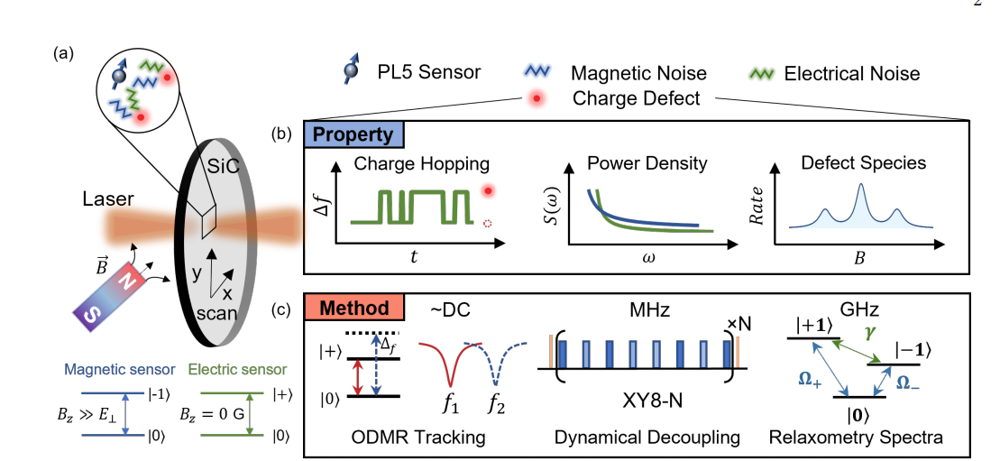
The article discusses the use of single PL5 centers in 4H-SiC as room-temperature broadband quantum sensors to study nanoscale charge defects in silicon carbide (SiC) at room temperature. It reports the first real-time observation of single-charge tunneling dynamics in a commercial semiconductor material and presents a comprehensive noise spectroscopy technique across various frequency bands (DC to GHz) using optically detected magnetic resonance (ODMR) and dynamical decoupling methods. The study provides insights into the local electric environment surrounding the PL5 centers and uncovers significant variations in noise spectra across different SiC wafer substrates.
Key findings include:
Real-Time Observation of Single-Charge Dynamics: The study demonstrates the ability to track charge tunneling events in SiC at room temperature, offering a novel approach for noise imaging and defect localization within semiconductors.
Noise Spectroscopy and Material Characterization: Different SiC wafers showed distinct noise environments, which can be linked to the defect density and material quality. The research highlights the role of charge defects in the local electric environment, significantly affecting the performance of semiconductor devices.
Nanoscale EPR Spectroscopy of Charge Defects: By utilizing the PL5 quantum sensors, the authors provided the first nanoscale electron paramagnetic resonance (EPR) spectroscopic fingerprint of charge defects in SiC, identifying silicon vacancies (V2) and other spin-1/2 defects as the primary sources of noise.
The study suggests that this method could be a valuable tool for optimizing SiC fabrication processes and improving defect engineering for semiconductor and quantum technologies, offering potential applications in characterizing third-generation semiconductors and advancing quantum information platforms.
The authors conclude that their approach has broader applications in characterizing quantum defects and their interactions, enabling precise diagnostics for wafer-level quality control in commercial SiC wafers.
OMeda (Shanghai Omedasemi Co.,Ltd) was founded in 2021 by 3 doctors with more than 10 years of experience in nanpfabrication. It currently has 15 employees and has rich experience in nanofabrication (coating, lithography, etching, two-photon printing, bonding) and other processes. We support nanofabrication of 4/6/8-inch wafers.