This article investigates the electro-optic (EO) properties of solution-processed Pb(Zr,Ti)O₃ (PZT) thin films, focusing on their potential for integration into silicon photonics. While Pb(Zr,Ti)O₃ is widely recognized for its electrical properties, its EO properties remain underexplored, limiting its use in electro-optic applications. The study highlights the fabrication of highly textured, fiber-oriented PZT films using a La₂O₂CO₃ template and chemical solution deposition (CSD) process, which is essential for ensuring compatibility with various photonic platforms.
Key findings from the study include:
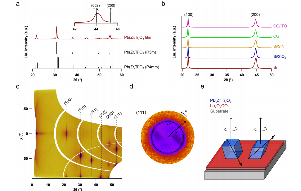
Film Fabrication and Properties:
The PZT films exhibit a strong rhombohedral crystal phase (R3m) with a fiber texture. The films have a low surface roughness (RMS = 0.73 nm) and a predominant (h00) out-of-plane orientation, which is beneficial for electro-optic applications.
The films are stabilized using a complexation process with Hacac (acetylacetone) to enhance the stability of the precursor solution.
Electro-Optic (EO) Characterization:
The films demonstrate a maximum Pockels coefficient (reff) of 68.98 pm/V and a remnant reff of 65.95 pm/V, showing strong and stable EO response, which is crucial for phase modulation applications.
The EO response is stable over time, with only minor transient phenomena observed in the first few hours after poling.
Device Integration:
The PZT films were integrated into a silicon nitride (SiN) O-band ring resonator. The resulting device exhibits a VπL product of 2.019 V·cm and a Pockels coefficient of 94.50 pm/V.
The ring resonator shows a linear wavelength shift in response to an applied voltage, with a tuning efficiency of 17.25 pm/V.
Material Performance:
The PZT thin films' performance compares favorably with state-of-the-art materials for electro-optic modulators, offering a high degree of polarization stability and low loss, making them suitable for use in high-speed, low-power photonic devices.
In conclusion, the solution-based approach to fabricating Pb(Zr,Ti)O₃ thin films, using a La₂O₂CO₃ template, offers a promising pathway for integrating this material into silicon photonics, particularly for applications in electro-optic modulators. The strong EO properties, high stability, and compatibility with photonic platforms make these films highly attractive for next-generation data communication systems.
OMeda (Shanghai Omedasemi Co.,Ltd) was founded in 2021 by 3 doctors with more than 10 years of experience in nanpfabrication. It currently has 15 employees and has rich experience in nanofabrication (coating, lithography, etching, two-photon printing, bonding) and other processes. We support nanofabrication of 4/6/8-inch wafers.