This article focuses on the development of a scalable gallium-phosphide-on-diamond (GaP-on-diamond) spin-photon interface, aimed at improving the performance and scalability of quantum networks. The key aspects and findings of the paper are as follows:
Background and Motivation:
Efficient coupling of quantum emitters (such as silicon-vacancy (SiV) centers in diamond) to nanophotonic cavities is crucial for the advancement of quantum networking. Traditional diamond-based photonic cavities face challenges in scalability and integration due to issues like surface defects and limited nonlinear properties of diamond.
GaP-on-Diamond Platform:
The study introduces a hybrid platform combining GaP photonic cavities integrated with diamond substrates. GaP offers a high refractive index and strong nonlinear properties, making it a promising material for integrated quantum photonics.
The approach involves fabricating GaP-on-diamond nanophotonic cavities that exhibit high cooperativity when coupled to SiV centers, which is essential for efficient spin-photon interactions required for quantum network applications.
Device Design:
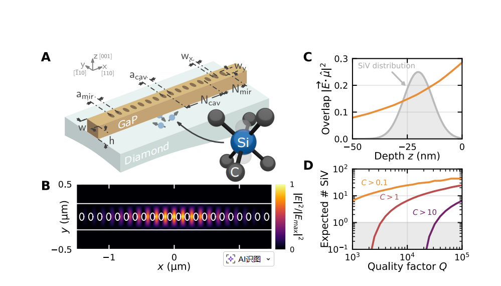
The design of the photonic cavity is optimized to maximize the cooperativity between the SiV centers and the cavity mode. The design involves a 1D GaP photonic crystal (PhC) nanobeam cavity integrated onto a planar diamond substrate. The geometry of the cavity is optimized to maximize both the cavity quality factor (Q) and the overlap of the cavity mode with the SiV spin transition.
Large-Scale Integration and Fabrication:
Over 4000 devices are fabricated on a 200 nm GaP membrane on AlGaP sacrificial layers, using electron-beam lithography (EBL) and reactive-ion etching. Devices are then transferred to a diamond substrate using a high-yield stamp-transfer method. The devices are shown to be highly reproducible, with a 99.5% yield.
High-Cooperativity Coupling:
The coupling between SiV centers and the GaP nanocavities is characterized at cryogenic temperatures (4 K). The system achieves a cooperativity greater than 1 (C > 1), which is crucial for efficient spin-photon interactions. The results indicate the successful realization of high-cooperativity coupling between quantum emitters and photonic cavities in a scalable platform.
Functional Demonstrations:
The paper demonstrates key functionalities such as spin-dependent optical transmission switching, where the cavity's transmission is modulated based on the spin state of the SiV center.
Single-shot readout of the SiV spin state is achieved, showing the ability to distinguish between spin states with high fidelity (96%).
Spin-Photon Interactions:
The article explores the spin relaxation times and quantum jumps of SiV centers, showing that the GaP-on-diamond interface allows for efficient spin-photon coupling and provides a robust platform for quantum information processing. The spin-relaxation time T1 of the SiV centers is measured to be around 420 µs.
Outlook and Potential:
This work highlights the potential of GaP-on-diamond as a scalable, high-performance platform for quantum networking. The strong nonlinear properties of GaP can be leveraged for on-chip quantum frequency conversion, integrated phononics, and cavity-optomechanics, opening up numerous possibilities for future quantum technologies.
In summary, the paper presents the GaP-on-diamond hybrid platform as a promising approach for scalable quantum networking, demonstrating high cooperativity coupling, efficient spin-photon interactions, and potential for integration with other quantum technologies.