The paper titled "Vertical and bevel-structured SiC etching techniques incorporating different gas mixture plasmas for various microelectronic applications" focuses on the fabrication of silicon carbide (SiC) etching techniques using inductively coupled plasma reactive ion etching (ICP-RIE). It investigates how different gas mixtures affect the etching of SiC substrates to create vertical and bevel structures, which are essential for various microelectronic devices like PIN diodes, Schottky diodes, and avalanche photodiodes (APDs).
Key findings include:
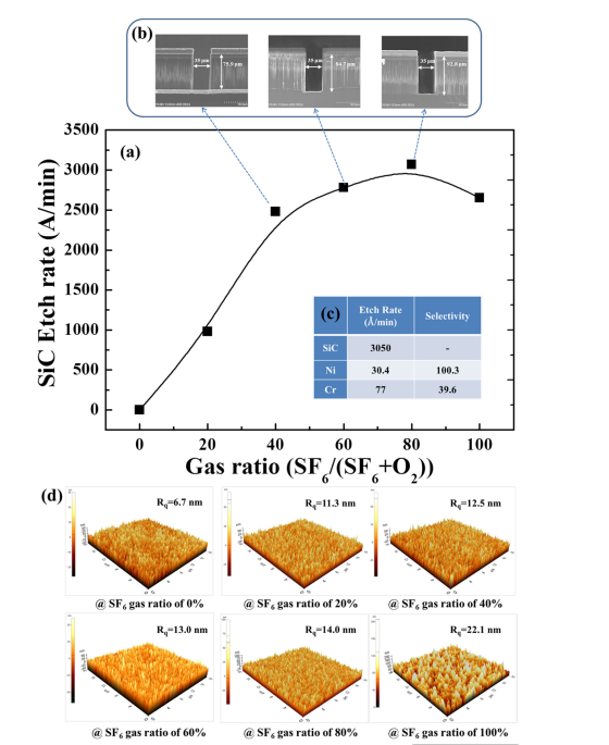
Vertical Etching: SF6 mixed with O2 was most effective for vertical etching, achieving the highest etching rate of 3050 Å/min. The study also explored the use of Ni and Cr masks for selectivity, with Ni showing better performance due to its higher selectivity.
Large-Angle Bevel Etching: For large-angle bevel etching, gas mixtures like BCl3 with N2 or Cl2 were tested. BCl3 + N2 showed a controllable etching angle range from 40° to 80°, which is ideal for fabricating devices like diodes and transistors. The optimal etching angle of approximately 60° is recommended for SiC-based devices.
Small-Angle Bevel Etching: For applications such as APDs, small-angle bevel etching (as low as 7°) is critical. The study found that Cl2 + O2 mixtures were most effective for achieving small bevel angles, with an etching rate of 411 Å/min and good selectivity.
The research demonstrates that SiC etching with these optimized gas mixtures can improve the performance and reliability of various microelectronic devices, including those with high breakdown voltages and low leakage currents. The results also emphasize the importance of adjusting gas mixtures to control etching angles and surface roughness for different applications.
OMeda (Shanghai Omedasemi Co.,Ltd) was founded in 2021 by 3 doctors with more than 10 years of experience in nanpfabrication. It currently has 15 employees and has rich experience in nanofabrication (coating, lithography, etching, two-photon printing, bonding) and other processes. We support nanofabrication of 4/6/8-inch wafers.