Paper Download

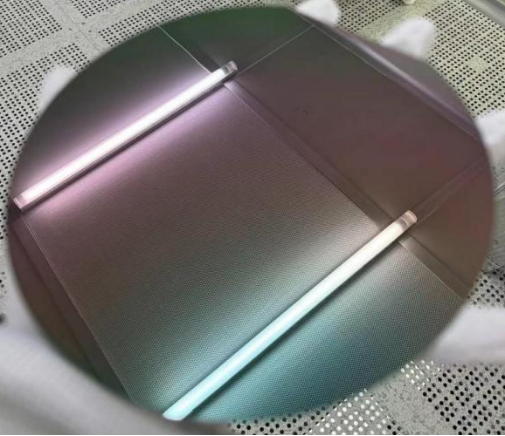
OMedaSemi can provide ultra low loss silicon nitride wafer , we use LPCVD/PECVD method to deposite Silicon Nitride film on thermal oxide wafer ,the film have good quality ,loss of thin film is 1dB/M,also the max size is 6 inch ,the max thickness is 800nm,we also have many stock ,you can visit this page to know more : Ultra Low Loss Silicon Nitride Thin Film Wafer

The article "Anneal-Free Ultra-Low Loss Silicon Nitride Integrated Photonics" presents a significant advance in the fabrication of ultra-low-loss silicon nitride (Si₃N₄) photonic integrated circuits (PICs) using a low-temperature, anneal-free process. The main highlights include:

1. **Low-Temperature Process**: The process uses a maximum temperature of 250°C, enabling compatibility with a wide range of materials and allowing the integration of Si₃N₄ with various low-temperature materials such as silicon electronics, III-V semiconductors, and organic materials.
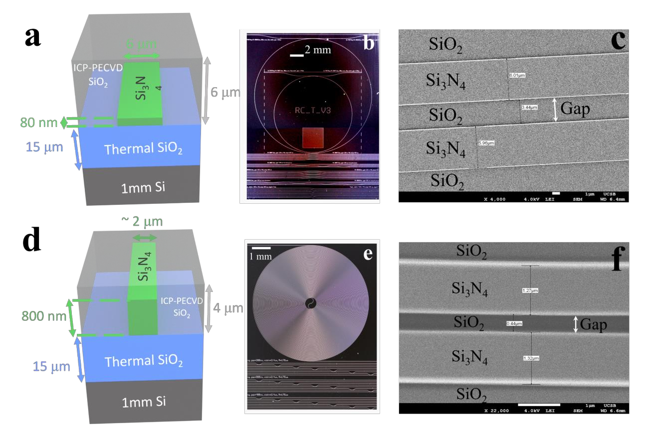
2. **Anneal-Free Fabrication**: This new method eliminates the need for high-temperature annealing, which was a previous barrier to heterogeneous and monolithic integration. The process also covers a range of Si₃N₄ core thicknesses from 80 nm to 800 nm without requiring stress mitigation or chemical mechanical polishing (CMP).
3. **Record-Low Loss**: The authors report achieving record-low losses of 1.77 dB/m for 80 nm nitride core waveguides and 8.66 dB/m for 800 nm thick nitride devices. These results represent a significant improvement over previously reported processes and set a new benchmark for silicon nitride PICs.
4. **Applications**: The process supports both linear and nonlinear photonic applications, such as laser frequency stabilization, optical parametric oscillation (OPO), and supercontinuum generation. Notably, it enables the integration of both thin and thick nitride devices, allowing for a wide range of applications in photonic circuits.
5. **Potential for Integration**: The anneal-free process opens up possibilities for heterogeneous integration with materials that cannot tolerate high temperatures, broadening the potential for advanced photonic and electronic systems integration.
This work marks a major step toward scalable, low-loss photonic circuits that can be integrated with a broader range of technologies, paving the way for future innovations in fields such as quantum computing, telecommunications, and sensing【17†source】 .
OMeda (Shanghai Omedasemi Co.,Ltd) was founded in 2021 by 3 doctors with more than 10 years of experience in nanpfabrication. It currently has 15 employees and has rich experience in nanofabrication (coating, lithography, etching, two-photon printing, bonding) and other processes. We support nanofabrication of 4/6/8-inch wafers.