OMedaSemi provides coated wafers for tantalum oxide optical waveguides and tantalum oxide superlenses.
Substrate
The substrate for the tantalum oxide thin film wafers used in superlenses is JGS1 fused silica glass.
The substrate for the tantalum oxide thin film wafers used in optical waveguides is a thermal oxide sheet. The thermal oxide layer thickness of the thermal oxide sheet is 3µm, but 4.7µm and 2µm thermal oxide layers are also available.
We offer thin films prepared by three deposition methods: electron beam evaporation, magnetron sputtering, and ion beam sputtering.
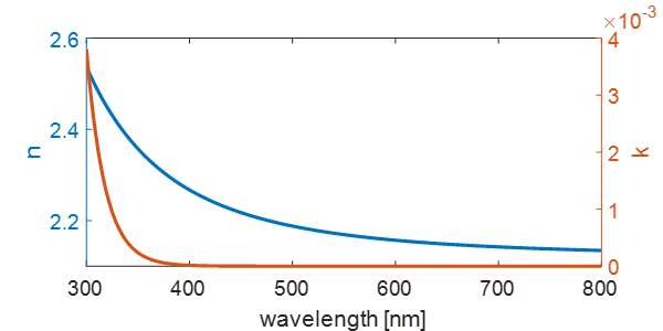
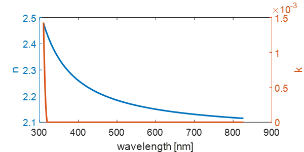
Their Refractive Index and absorption are as follows:
Electron beam evaporation: 5 6-inch wafers per batch; lowest coating cost, but the film has high optical absorption and high loss.
 Ta2O5 Magenetron sputtering leybold helios 800.xlsx
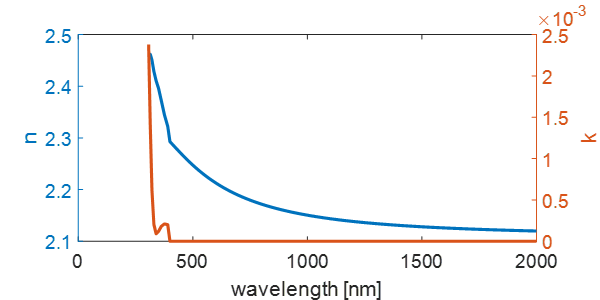
Magnetron sputtering: 11 8-inch wafers per batch; high coating cost, medium optical absorption, medium loss.
 N&K of Ta2O5 by Magentron Sputtering.png
Ion beam sputtering, producing four 6-inch wafers in one batch, high coating cost, high film quality, low optical absorption, and low loss.
OMeda (Shanghai Omedasemi Co.,Ltd) was founded in 2021 by 3 doctors with more than 10 years of experience in nanpfabrication. It currently has 15 employees and has rich experience in nanofabrication (coating, lithography, etching, two-photon printing, bonding) and other processes. We support nanofabrication of 4/6/8-inch wafers.