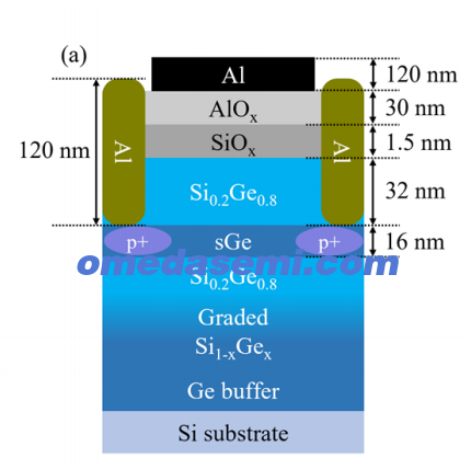
12inch Strained GeOI Wafer Product Information:
(1) Device Layer:
Thickness: 15nm
Device Layer Composition: Si0.25Ge0.75~Pure Ge Doping: w/o doping (P-type)
Strain: Compressive, -1.6%@Si0.25Ge0.75
Defect Density:<1E15 cm-3
Surface Roughness:<1nm
(2) BOX Layer
Material: SiO2
Thickness: 20nm
(3)Handle Wafer:SIlicon 775um P100 1-100ohm*cm SSP
We also offer other types of GEOI products:
MOS, Quantum, FinFET:
Strained germanium wafers/Unstrained germanium wafers
Silicon photonics:
Germanium epitaxial wafers on silicon waveguides for silicon germanium detectors (Naura Technology Group equipment, max 12 inch)
Mid- and far-infrared germanium waveguides: GeOi wafers:

Semiconductor equipment manufacturers, wet chemical plants:
Epiaxial germanium wafers of different compositions
5% 10% 15% 20% 25% 30% 50% 75% 100% germanium epitaxial substrates, max 12 inch
OMeda (Shanghai Omedasemi Co.,Ltd) was founded in 2021 by 3 doctors with more than 10 years of experience in nanpfabrication. It currently has 15 employees and has rich experience in nanofabrication (coating, lithography, etching, two-photon printing, bonding) and other processes. We support nanofabrication of 4/6/8-inch wafers.