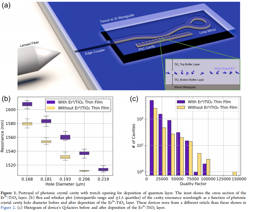
The article "Monolithically Integrated C-Band Quantum Emitters on Foundry Silicon Photonics" demonstrates the integration of erbium-doped titanium dioxide (Er3+:TiO2) thin films on a silicon photonic platform to create single-photon emitters in the telecom C-band. This work utilizes a scalable approach, fabricating high-quality photonic crystal nanobeam cavities using a 300 mm CMOS-compatible foundry platform. These cavities are then interfaced with erbium ions through backend deposition of TiO2 thin films, which enhance optical emission through the Purcell effect.
The research focuses on improving the coupling efficiency of these devices by varying parameters like hole diameter and coupling gap size. The results show that erbium ions in TiO2 thin films exhibit Purcell enhancement factors up to 500, and single photon emission was confirmed through photon autocorrelation measurements, demonstrating potential for quantum networking applications. The platform’s integration with foundry processes offers a pathway to scalable, manufacturable quantum devices, making it suitable for future developments in quantum repeaters, interconnects, and telecom systems .
OMeda (Shanghai Omedasemi Co.,Ltd) was founded in 2021 by 3 doctors with more than 10 years of experience in nanpfabrication. It currently has 15 employees and has rich experience in nanofabrication (coating, lithography, etching, two-photon printing, bonding) and other processes. We support nanofabrication of 4/6/8-inch wafers.

