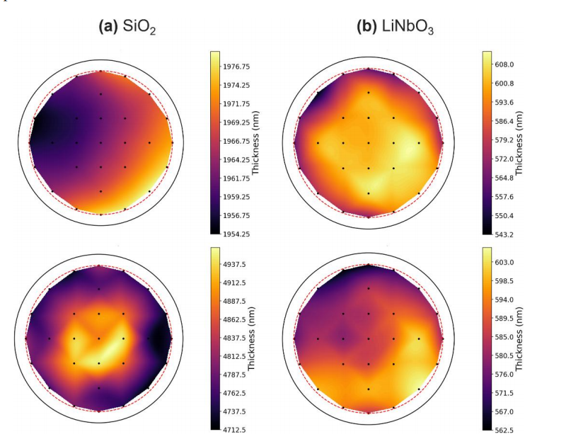
This study reports the fabrication and comprehensive characterization of 6-inch X-cut lithium niobate on insulator (LNOI) wafers, produced at CEA-Leti using the Smart Cut technique. Thin-film lithium niobate (TFLN) is a promising platform for integrated photonics due to its high electro-optic, acousto-optic, and nonlinear optical properties, as well as low propagation losses and wide transparency range. The Smart Cut process combines ion implantation, wafer bonding, and chemical-mechanical polishing, producing high-quality TFLN layers with 600 nm thickness and high thickness uniformity (±3–5%), and sub-nanometer surface roughness (0.17 nm RMS) suitable for photonic integrated circuits (PICs).
Structural analyses using AFM, SEM, TEM, and X-ray diffraction confirmed smooth, defect-free LiNbO3 films with high crystallinity and uniform SiO2 buffer layers of either 1.9 µm (thin-BOX) or 4.8 µm (thick-BOX), providing high optical confinement. Ellipsometry verified refractive indices consistent with bulk values (n_o ≈ 2.21–2.29, n_e ≈ 2.13–2.21) and high index contrast with SiO2, ensuring efficient waveguiding.
Optical characterization of ridge waveguides fabricated on these wafers revealed extremely low propagation losses (<0.5 dB/cm) and high electro-optic efficiency, with a Mach-Zehnder modulator achieving a half-wave voltage-length product Vπ•L of 2.38 ± 0.06 V·cm at 1550 nm, demonstrating high-speed modulation capabilities. The wafers combine structural perfection and optical performance, making them suitable for advanced integrated photonic and quantum devices, including modulators, resonators, and high-Q photonic circuits. The study highlights the potential for scalable European fabrication of high-quality LNOI wafers for next-generation photonic applications.
OMeda (Shanghai Omedasemi Co.,Ltd) was founded in 2021 by 3 doctors with more than 10 years of experience in nanpfabrication. It currently has 15 employees and has rich experience in nanofabrication (coating, lithography, etching, two-photon printing, bonding) and other processes. We support nanofabrication of 4/6/8-inch wafers.