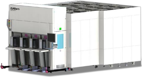
SAB8210CW--Fully automatic C2W chip bonding machine
| Pressure range | 1~300N |
Post-bonding accuracy | ≤±1μm;≤±500nm, ≤±200nm@3σ |
Chip SIZE | 1*1~50*50mm |
Wafer SIZE | Φ200mm、Φ300mm |
TF Workstation | 2 |
FOUP station | 2 |
UPH | 400~2000 |
Process Capabilities | Cu-SiO2 mixed bonding; Cu/SiCN mixed bonding |
Multi-module integrated | Activation, cleaning, UV treatment, top extraction, alignment, bonding, and detection |
OMeda (Shanghai Omedasemi Co.,Ltd) was founded in 2021 by 3 doctors with more than 10 years of experience in nanpfabrication. It currently has 15 employees and has rich experience in nanofabrication (coating, lithography, etching, two-photon printing, bonding) and other processes. We support nanofabrication of 4/6/8-inch wafers.