This work demonstrates highly efficient, integrated quantum memories for light based on Eu³⁺:Y₂SiO₅ crystals coupled with impedance-matched microcavities, achieving unprecedented storage performance for solid-state photonic systems. Two distinct architectures are implemented:
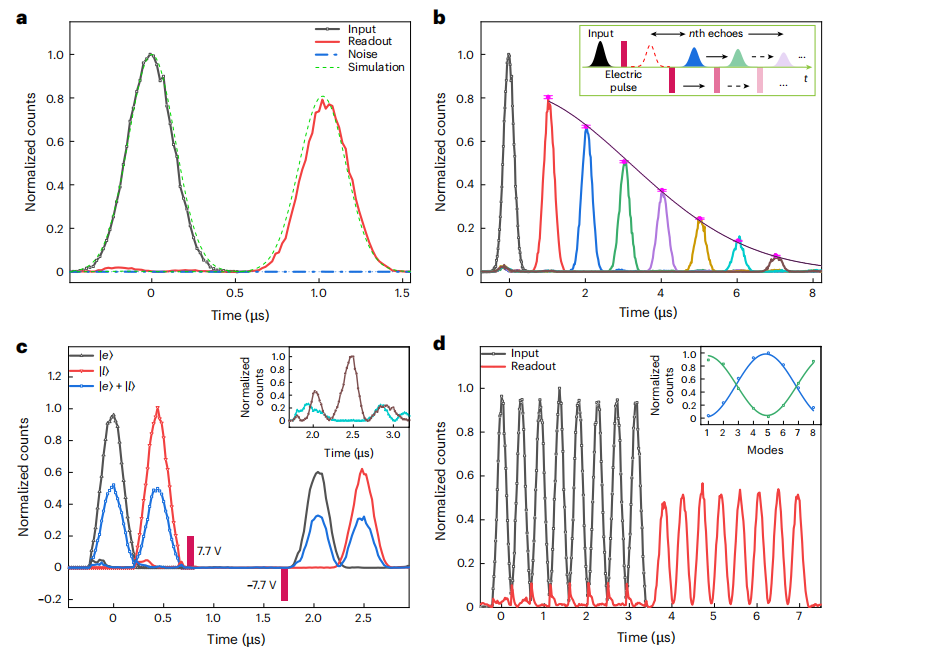
Waveguide cavity (WGC): Fabricated by applying reflective coatings on a femtosecond laser-written optical waveguide with on-chip coplanar electrodes. It enables on-demand readout via Stark-shift-induced interference and achieves 80.3% storage efficiency for single-photon-level weak coherent pulses, surpassing all previously reported integrated quantum memories. Eight temporal modes are stored with an average efficiency of 52.9% over 3.8 µs.
Fibre-based cavity (FBC): Employs a 200 µm Eu³⁺:Y₂SiO₅ membrane integrated with a concave fibre mirror and sapphire substrate. It achieves 69.8% storage efficiency for telecom-heralded single photons, stores 20 temporal modes with an average efficiency of 51.3% over 10 µs, and allows spectral tuning over a 10 GHz range via variable strain in the thin membrane (see Fig. 3d, page 5).
Both architectures preserve quantum coherence with fidelities exceeding 99% and interference visibilities of ~0.94 for multiple temporal modes. The FBC provides a spectrally tunable, wideband interface for quantum light sources, while the WGC allows high-density on-chip integration and potential spatial multiplexing. Heralded single-photon experiments in the C-band confirm non-classical correlations with a cross-correlation of 16.4, setting a new benchmark for solid-state single-photon storage (Fig. 4, page 5).
The work demonstrates multiplexed quantum storage surpassing the no-cloning efficiency limit of 50% with extremely small device volumes (~4 × 10⁻⁵ mm³), offering a practical platform for scalable quantum networks, photonic processors, and quantum repeaters (Fig. 5, page 5). The combination of high efficiency, multimode capacity, spectral tunability, and compact integration represents a significant advance over prior solid-state and cold-atom memories.
OMeda (Shanghai Omedasemi Co.,Ltd) was founded in 2021 by 3 doctors with more than 10 years of experience in nanpfabrication. It currently has 15 employees and has rich experience in nanofabrication (coating, lithography, etching, two-photon printing, bonding) and other processes. We support nanofabrication of 4/6/8-inch wafers.