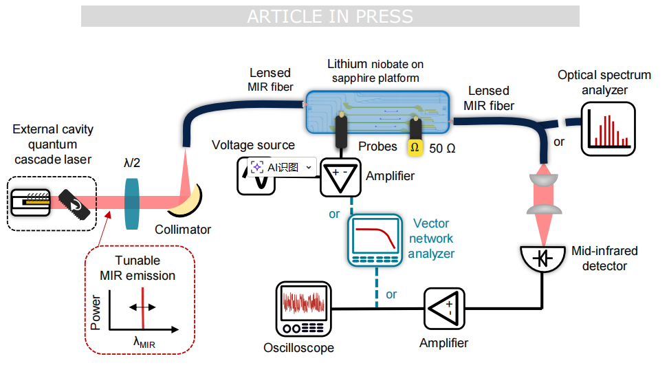
This study demonstrates the first integrated electro-optic modulator for the mid-infrared (MIR) range based on thin-film lithium niobate on sapphire (LNOS), addressing the limitations of LNOI (lithium niobate on insulator) platforms, which suffer from SiO₂ absorption beyond ~3.4 µm. The device is a traveling-wave Mach–Zehnder interferometer (MZM), designed for operation near 4 µm, with broad tunability from 3.95 to 4.5 µm.
Key performance metrics include: a half-wave voltage–length product (VπL) of 22 V·cm, a 3-dB electro-optic bandwidth exceeding 20 GHz, an extinction ratio of 17 dB, and optical output power above 350 µW. Two LN film thicknesses, 0.9 µm and 1.5 µm, were evaluated, revealing that thicker films improve optical confinement, reduce Vπ, and allow electrodes to be placed closer without excessive plasmonic loss. Propagation loss is low (~1.1 dB/cm at 4 µm), dominated by sidewall roughness, and total fiber-to-fiber insertion loss ranges from 14–24 dB across the measured spectrum.
The modulator enables 10 Gbit/s free-space optical transmission and generates a 70 GHz frequency comb through amplitude modulation, demonstrating its suitability for MIR spectroscopy, high-speed communication, and frequency-comb generation. Fabrication uses electron-beam lithography, argon RIE etching, gold electrode deposition, and focused ion beam facet milling to achieve precise control, low-loss waveguides, and high reproducibility. Sapphire provides excellent thermal management, transparency in the MIR, and low RF losses, making it a promising platform for scalable, high-performance MIR photonics.
In summary, this work establishes LNOS as a viable platform for compact, high-speed, and low-loss mid-infrared modulators, unlocking capabilities for integrated MIR coherent sensing, spectroscopy, and free-space communication that were previously inaccessible with conventional LNOI or semiconductor platforms .
OMeda (Shanghai Omedasemi Co.,Ltd) was founded in 2021 by 3 doctors with more than 10 years of experience in nanpfabrication. It currently has 15 employees and has rich experience in nanofabrication (coating, lithography, etching, two-photon printing, bonding) and other processes. We support nanofabrication of 4/6/8-inch wafers.