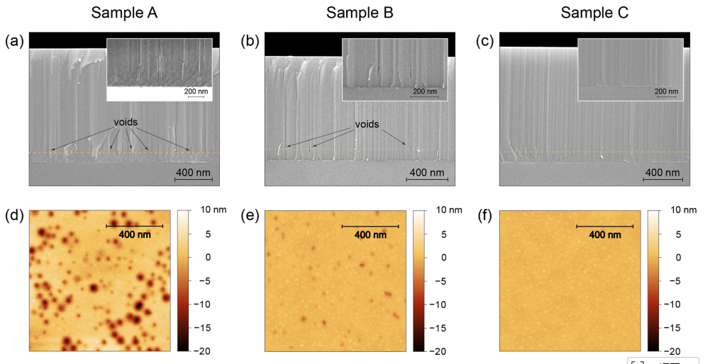
This work addresses optical losses in aluminum nitride (AlN) photonic integrated circuits (PICs) on sapphire, focusing on the detrimental impact of voids commonly found in MOVPE-grown AlN layers. Void-containing layers exhibit propagation losses exceeding 30 dB/cm at 1550 nm, as confirmed experimentally on waveguides and microring resonators (MRRs) and supported by FDTD simulations that reveal strong scattering dependent on void size, height, and density. Smaller voids, negligible at telecom wavelengths, can still produce significant losses in visible and UV regimes due to the λ⁻⁴ scaling of volumetric scattering (Figures 6–7, pages 6–7) .
To mitigate this issue, the authors introduce a thin sputtered AlN buffer layer prior to MOVPE growth, resulting in void-free hybrid AlN layers. These layers achieve intrinsic quality factors (Qint) up to 2 × 10⁶ in microring resonators at 1550 nm, corresponding to propagation losses below 0.2 dB/cm, a two-orders-of-magnitude improvement over standard MOVPE-grown layers (Table 2, page 5). Nonlinear optical performance is validated through on-chip second-harmonic generation (SHG) and supercontinuum generation (SCG) in dispersion-engineered waveguides, demonstrating suitability for high-power and short-wavelength photonic applications (Figures 8–9, pages 8–9).
The study shows that hybrid AlN-on-sapphire layers with a sputtered buffer provide a scalable, high-quality platform for low-loss integrated photonics, particularly advantageous for visible and UV photonic circuits, where scattering losses are most critical. The approach ensures high material uniformity, minimizes defects, and supports both linear and nonlinear photonic functionalities, opening paths for advanced integrated optical devices with applications in quantum photonics, visible-light PICs, and nonlinear optics .
OMeda (Shanghai Omedasemi Co.,Ltd) was founded in 2021 by 3 doctors with more than 10 years of experience in nanpfabrication. It currently has 15 employees and has rich experience in nanofabrication (coating, lithography, etching, two-photon printing, bonding) and other processes. We support nanofabrication of 4/6/8-inch wafers.