This study investigates the mechanism of N₂ plasma activation for SiO₂ wafer bonding at low temperatures, a process critical for MEMS and IC packaging. Nitrogen plasma is applied to SiO₂ surfaces to enhance wafer-to-wafer (W2W) bonding, increasing surface hydrophilicity and bonding strength while reducing processing temperature to 300 °C, avoiding thermal damage to sensitive devices. The work combines experiments, finite element analysis (FEA) of a capacitively coupled plasma (CCP) chamber, and molecular dynamics (MD) simulations to elucidate the atomic-scale mechanisms underlying bonding enhancement.
Key findings include:
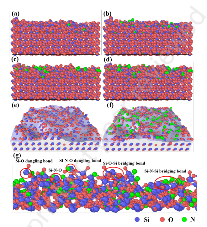
Optimal plasma bias power (60 W) maximizes surface hydroxylation, yielding a contact angle of 1.51° and the highest bonding energy of 1.549 J/m². Lower powers produce insufficient surface activation, while higher powers (≥80 W) cause surface reconstruction, depletion of dangling bonds, and formation of inert Si–N (or O)-Si bridging bonds, reducing wettability and bond strength.
FEA simulations reveal that increasing plasma power elevates electron temperature, ion flux, and incident ion energy, which are used as input for MD simulations to replicate realistic surface modifications over experimental timescales.
MD simulations demonstrate that N₂ plasma breaks Si–O bonds, forms active dangling bonds (Si–O, Si–N), and promotes adsorption of hydroxyl groups. These changes facilitate strong hydrogen bonding with water molecules, enhancing surface hydrophilicity and interfacial bonding. Excessive plasma exposure, however, induces inactive bridging bonds and surface roughening, reducing bonding efficiency.
The correlation between active-to-inactive site ratio, surface roughness, and bonding strength provides a mechanistic understanding of how plasma parameters govern W2W adhesion. Simulations align closely with experimental contact-angle measurements and bonding tests, validating the computational approach.
The study establishes a predictive framework for selecting nitrogen plasma activation parameters to optimize SiO₂ wafer bonding at low temperatures, combining experimental and computational insights to improve process efficiency, reduce trial-and-error, and guide MEMS and photonic packaging strategies.
OMeda (Shanghai Omedasemi Co.,Ltd) was founded in 2021 by 3 doctors with more than 10 years of experience in nanpfabrication. It currently has 15 employees and has rich experience in nanofabrication (coating, lithography, etching, two-photon printing, bonding) and other processes. We support nanofabrication of 4/6/8-inch wafers.