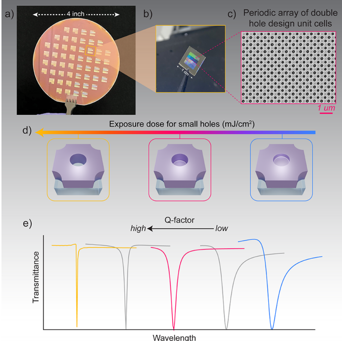
This work demonstrates the wafer-scale fabrication of high-Q all-dielectric quasi-bound states in the continuum (qBIC) metasurfaces using deep-ultraviolet lithography (DUVL), overcoming the scalability and throughput limitations of conventional electron-beam lithography. The metasurfaces are patterned in 160 nm silicon nitride (Si₃N₄) on silica wafers with a double-hole C4-symmetry-broken unit cell, where small-hole radius and depth are controlled to tune the Q-factor of the qBIC resonances (Figures 1–3, pages 2–4).
Key findings include:
Q-factor engineering via dual-parameter control: The Q-factor can be tuned by adjusting small-hole radius asymmetry (Δr) and exposure-dose-controlled hole depth. Fully etched small holes achieve simulated Q-factors ∼2600, while shallow or stochastic holes yield lower Q, providing a practical pathway for tailoring resonance properties within DUVL resolution limits.
Nonlocal resonance robustness: qBIC modes show spatial uniformity across the wafer, despite stochastic nanoscale variations in hole depth, because the modes arise from collective coupling across multiple unit cells (Figures 4a–l, page 6). This nonlocality relaxes lithography tolerances and enables high-throughput manufacturing.
Refractive index sensing: The wafer-scale metasurfaces achieve 129 nm/RIU sensitivity, validated via exposure to aqueous glycerol solutions (0–50%), with linear spectral redshifts and high-fidelity CMOS camera-based readout. Single-wavelength intensity interrogation combined with hyperspectral imaging provides effective sample discrimination even at modest refractive index changes (Figure 5, page 6–7).
Scalable nanofabrication: DUVL enables full-wafer patterning within 1–2 minutes, producing multiple chips per wafer with sub-200 nm features, making the approach suitable for commercial biosensing arrays, on-chip spectroscopy, and integrated photonic systems.
Overall, the study establishes a practical, CMOS-compatible platform for high-Q dielectric qBIC metasurfaces, combining high performance, spatial uniformity, and manufacturability, bridging the gap between nanophotonic design and scalable semiconductor fabrication. This enables deployment of metasurface-based biosensors, spectrometers, and integrated photonics in real-world applications.
OMeda (Shanghai Omedasemi Co.,Ltd) was founded in 2021 by 3 doctors with more than 10 years of experience in nanpfabrication. It currently has 15 employees and has rich experience in nanofabrication (coating, lithography, etching, two-photon printing, bonding) and other processes. We support nanofabrication of 4/6/8-inch wafers.