This work presents ultra-compact, high-electromechanical-coupling lithium niobate (LN) thin-film bulk acoustic wave resonators (FBARs) operating in the 10–30 GHz millimeter-wave range, addressing limitations of prior AlN/ScAlN FBARs and lateral-field LN XBARs. Unlike previous LN FBARs requiring pre-patterned bottom electrodes, the authors demonstrate a thickness-field-excited (TFE) LN FBAR using a single top and bottom electrode configuration, optimizing electrode thickness to co-optimize first-order (S1) and third-order (S3) symmetric modes (pages 2–3).
Key experimental results include: S1 mode at 10.5 GHz with Qₛ = 38 and k² = 14.1%, and S3 mode at 26.8 GHz with Qₛ = 22 and k² = 11.3% (pages 4–5). The devices are fabricated using ion milling, SiO₂ backfill, metal electrode deposition, and XeF₂ release of the a-Si sacrificial layer, yielding 50-Ω matched devices with footprints as small as 70 µm² at 26.8 GHz—nearly ten times smaller than LN XBARs at similar frequencies (page 4). Material characterization using BF-STEM and XRD confirms high-quality single-crystal 36° Y-cut LN, Al electrodes, and a-Si sacrificial layers (page 3–4).
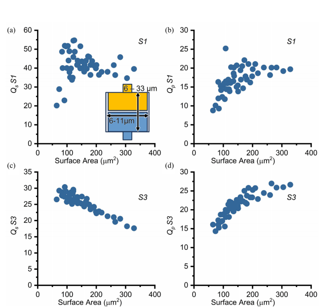
Performance studies include lateral dimension sweeps, showing Q dependence on surface area due to energy confinement, power-handling analysis demonstrating stable S1 performance up to ~9 dBm and S3 up to ~3.8 dBm, and temperature coefficient of frequency (TCF) measurements, revealing negative TCF values ranging from −96 to −160 ppm/K (pages 5–6). Compared to state-of-the-art LN FBARs, this platform achieves higher operating frequencies, competitive k², compact footprint, and fs·Qs products up to 5.9 × 10¹¹, demonstrating the potential for compact millimeter-wave acoustic filters (page 7).
In conclusion, this study establishes TFE LN FBARs as a scalable, high-coupling, and miniature acoustic platform for cmWave and mmWave applications, with design strategies—such as piezoelectric-to-metal volume ratio optimization and electrode geometry tuning—enabling further improvements in Q, k², and overall figure of merit
OMeda (Shanghai Omedasemi Co.,Ltd) was founded in 2021 by 3 doctors with more than 10 years of experience in nanpfabrication. It currently has 15 employees and has rich experience in nanofabrication (coating, lithography, etching, two-photon printing, bonding) and other processes. We support nanofabrication of 4/6/8-inch wafers.