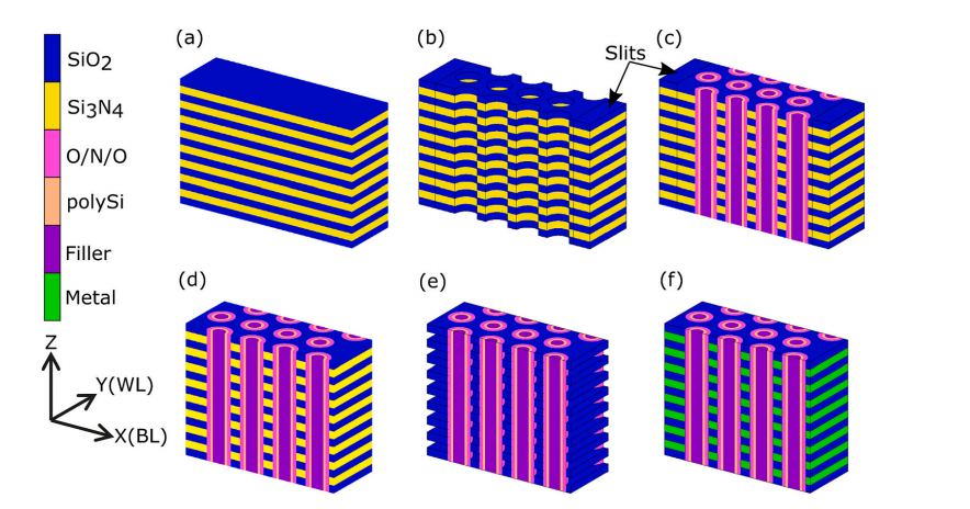
This study addresses wafer warpage in 3-D NAND flash memory fabrication, which is a critical challenge as the number of vertically stacked layers increases. Excessive warpage can cause mechanical stress, pillar bending, layer collapse, overlay misalignment, and lithography errors, limiting scalability. The authors use a multi-scale finite-element modeling (FEM) approach, integrating local device-level simulations into wafer-level global simulations, to track residual stresses and deformation throughout the fabrication process (pages 2–3, Figures 1–2).
Key findings include:
Sources of warpage: Sequential depositions of SiO₂/Si₃N₄ layers generate biaxial compressive stresses (~−110 MPa), while subsequent memory hole etching and slit etching induce stress relaxation and anisotropy, leading to saddle-shaped, radially asymmetric warpage with maximum differences between word-line (WL) and bit-line (BL) directions of up to ~294 μm (pages 3–4, Figures 4–5).
Slit pitch optimization: Increasing horizontal slit pitch reduces stress anisotropy, confining lateral relaxation more uniformly. For instance, increasing the pitch from 0.78 μm to 9.52 μm decreases stress asymmetry to ~7 MPa and mitigates the saddle-shaped deformation (pages 5, Figures 5–6).
Metal and oxide layer scaling: Reducing metal layer thickness (from 25 nm to 15 nm) while keeping oxide thickness constant decreases stress anisotropy, especially when using low-stress Ruthenium (Ru) instead of Tungsten (W). With Ru, residual stresses drop below 10 MPa, producing near-symmetric wafer deformation (pages 6–7, Figures 7–9).
Passivation layer effects: Thinner or low-stress passivation layers, particularly Si₃N₄ with mild tensile stress, further reduce warpage uniformly in both WL and BL directions. Combining optimized metal, passivation, and thickness strategies can reduce wafer warpage below 10 μm for a 128-layer 3-D NAND stack, providing a mechanically scalable path forward (pages 7–8, Figures 10–13).
The study concludes that a sequential strategy—first achieving symmetric deformation via low-stress metal selection, then applying isotropic mitigation via passivation control—offers a robust, scalable solution for minimizing warpage and asymmetry in advanced 3-D NAND technology, enabling continued vertical scaling without mechanical limitations (page 8, Conclusions).
OMeda (Shanghai Omedasemi Co.,Ltd) was founded in 2021 by 3 doctors with more than 10 years of experience in nanpfabrication. It currently has 15 employees and has rich experience in nanofabrication (coating, lithography, etching, two-photon printing, bonding) and other processes. We support nanofabrication of 4/6/8-inch wafers.