This study reports the fabrication of InP-based vertical-cavity surface-emitting lasers (VCSELs) using wafer bonding with a fast atomic beam (Ar-FAB) activated silicon interlayer. The introduction of a 7 nm Si interlayer at the GaAs/InP bonding interface significantly improves bonding strength while minimizing optical absorption losses at the interface, enabling efficient current-injection lasing at 1380 nm under continuous-wave operation. The VCSELs demonstrate mill watt-level optical output power from a single emitter and maintain stable operation up to 110 °C (pages 2–5).
The fabrication process involves:
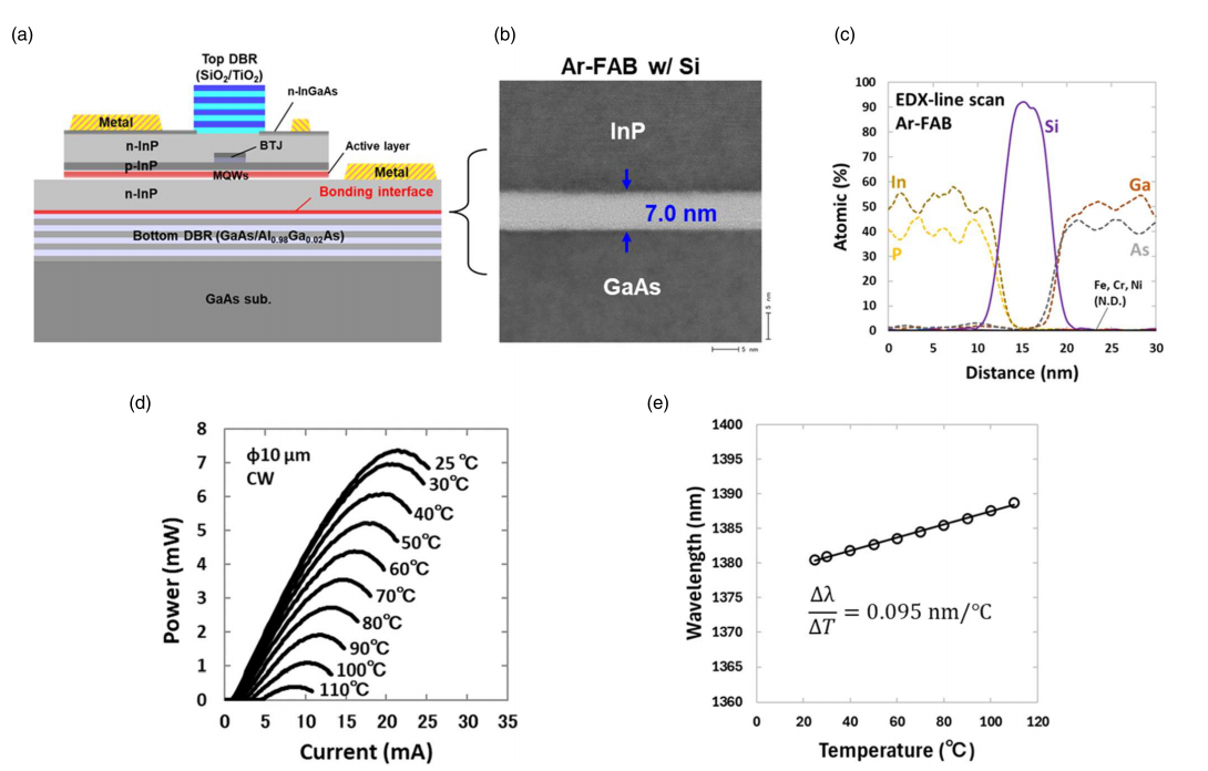
Activation of InP and GaAs surfaces with Ar-FAB, followed by sputtering of Si atoms onto both surfaces.
Direct wafer bonding under pressure, forming a void-free, sharply defined bonding interface validated by STEM and EDX analysis (Figures 2b–c, page 4).
Growth of the bottom DBR (30 pairs of GaAs/Al₀.₉₈Ga₀.₀₂As) and InP-based active region with buried tunnel junctions (BTJs), followed by electrode deposition and top DBR coating.
Device characterization shows that the Ar-FAB + Si VCSELs outperform ionized Ar bonded VCSELs, which exhibit heavy metal contamination (Fe, Cr, Ni) at the interface, higher optical absorption, lower slope efficiency, and reduced thermal performance (Figures 4–5, pages 5–6). The lasing wavelength exhibits a temperature dependence of 0.095 nm/°C, consistent with prior bonded VCSELs.
The results demonstrate that Ar-FAB activation combined with a thin Si interlayer allows low-temperature, high-strength bonding of dissimilar materials (GaAs and InP) while preserving optical quality, providing a scalable approach for heterogeneous integration in silicon photonics, data communication, and 3D sensing applications (page 7).
OMeda (Shanghai Omedasemi Co.,Ltd) was founded in 2021 by 3 doctors with more than 10 years of experience in nanpfabrication. It currently has 15 employees and has rich experience in nanofabrication (coating, lithography, etching, two-photon printing, bonding) and other processes. We support nanofabrication of 4/6/8-inch wafers.