This study reviews the die-to-wafer (D2W) hybrid and fusion bonding processes for advanced 3D integration in high-bandwidth memory (HBM) and CMOS image sensor (CIS) applications. As chiplet heterogeneous integration scales from low-volume to high-volume manufacturing, D2W bonding faces challenges in tool and process integration, yield optimization, placement accuracy, and overlay metrology.
Key innovations and findings include:
TEL Clean Carrier (TCC): A reusable 300 mm substrate carrier designed to replace conventional tape-frame carriers. The TCC ensures die retention, chemical resistance, plasma and vacuum compatibility, and minimal ESD risk, enabling defect-free handling of ultra-thin dies (30–50 µm) and large dies up to 30 × 30 mm². Post-die ejection treatments restore surface topography for multiple reuses (pages 3–4, Figures 3–4, Tables 1–2).
Cluster Tool Integration: A modular cluster tool accommodates the TCC, combining surface preparation (wet and plasma), D2W bonding, and optional in-line metrology. This system maintains compact footprint and leverages existing plasma and wet chambers without scaling for tape-frame handling (pages 4–5, Figures 2).
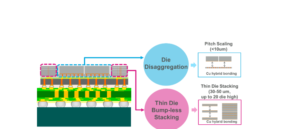
Bonding Results: Successful bonding of blanket dielectric and patterned die with pitches down to 4.5 µm was demonstrated. High-yield bonding was achieved for ultra-thin dies (30 µm), large dies (30 × 30 mm²), and multi-die stacks up to 4–8 layers. C-SAM inspection confirmed void-free interfaces for most conditions, although systematic voids from saw-dicing defects were noted, highlighting the need for plasma dicing to improve yield (pages 5–8, Figures 5–10).
Placement Accuracy and Overlay: Scaling die bond pads to 3 µm or sub-1 µm requires placement accuracy of 50 nm and alignment accuracy <40 nm. Subsystem analysis identified vision systems (40%), bond head stability (40%), and precision stages (20%) as major contributors to overlay error. Learning from lithography overlay and scanner control is critical for next-generation bonder design (pages 8–10, Tables 4–5).
Advanced Metrology: Conventional IR-based overlay metrology has depth-of-focus and metal-penetration limitations. The study introduces multi-modal X-ray metrology with Moiré fiducials, enabling nm-scale overlay measurement for multi-die stacks in HBM applications. Initial feasibility tests confirm that Moiré amplification can translate micron-scale shifts into 10s-of-nm-level overlay measurements (pages 10–11, Figures 11–12).
In summary, the paper presents a holistic approach to D2W bonding, integrating a reusable TCC, cluster tool workflow, die stacking capability, next-generation placement control, and novel X-ray overlay metrology. These developments address critical challenges in yield, accuracy, and high-volume manufacturability for advanced 3D chiplet integration.
OMeda (Shanghai Omedasemi Co.,Ltd) was founded in 2021 by 3 doctors with more than 10 years of experience in nanpfabrication. It currently has 15 employees and has rich experience in nanofabrication (coating, lithography, etching, two-photon printing, bonding) and other processes. We support nanofabrication of 4/6/8-inch wafers.