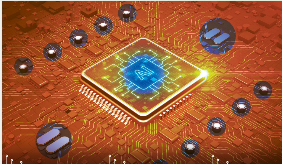
The article presents a roadmap for advanced semiconductor packaging to 2030, focusing on heterogeneous integration of logic, memory, photonics, and substrates to support the growing demands of artificial intelligence (AI) and high-performance computing (HPC). Key trends include:
Chiplet-based 3D Integration: Large monolithic SoCs are being replaced by modular chiplets connected via 3DIC stacking, through-silicon vias (TSVs), hybrid bonding, and backside power delivery networks (PDNs). This improves yield, scalability, power efficiency, and design flexibility.
High-Bandwidth Memory (HBM): Memory evolution from HBM3E to HBM5 aims to overcome the “memory wall,” delivering >4 TB/s bandwidth through ultradense stacking and direct metal–metal bonding. Thermal management, thin-die handling, and precise alignment are critical for reliability and performance.
Copackaged Optics (CPO): Integrating photonic engines with compute dies addresses interconnect bandwidth and energy limits. CPO enables >100 Tb/s bandwidth with reduced latency and power per bit. Precise alignment, thermal management, and mixed-signal co-design are necessary for large-scale deployment.
Interposers and Advanced Substrates: Scaling lateral interposer dimensions beyond 8× reticle sizes, with organic and glass cores, supports more dies, higher density, and better electrical and thermal performance. Panel-level packaging (PLP) enhances throughput and cost efficiency.
Low-Temperature Hybrid Bonding: Hybrid bonding with nitrogen-doped carbide (NDC) dielectrics and fine-grain (FG) copper allows sub-10 nm interconnect pitches, enabling reliable, high-density, solderless connections for HBM and heterogeneous integration. NDC provides strong Cu diffusion barriers, excellent hermeticity, and low outgassing, while FG Cu ensures bond integrity at lower temperatures.
Thermal Management: AI/HPC workloads can exceed 2–5 kW, requiring innovations such as microfluidic cooling, TIMs with graphene or diamond, and thermally-aware chiplet placement to maintain uniform temperatures and prevent hot spots.
The article emphasizes that advanced packaging has evolved from a mechanical necessity to a system-level performance enabler, driving energy-efficient, scalable, and high-bandwidth computing systems. Integration, thermal management, low-temperature bonding, and material innovations collectively support the next generation of AI and HPC systems.
OMeda (Shanghai Omedasemi Co.,Ltd) was founded in 2021 by 3 doctors with more than 10 years of experience in nanpfabrication. It currently has 15 employees and has rich experience in nanofabrication (coating, lithography, etching, two-photon printing, bonding) and other processes. We support nanofabrication of 4/6/8-inch wafers.