The article reviews the heterogeneous integration of thin-film lithium niobate (TFLN) onto silicon photonics (SiPho) platforms using micro-transfer printing (μTP), emphasizing its potential for scalable, high-performance photonic devices. Silicon and silicon nitride waveguides provide mature, high-volume fabrication capabilities, while lithium niobate offers superior electro-optic properties and strong nonlinearities, enabling high-speed modulation, second-harmonic generation, and quantum photonics.
The review compares different integration strategies:
Wafer-to-wafer and die-to-wafer bonding: Mature techniques offering scalable and uniform integration, suitable for batch processing but requiring smooth surfaces and higher thermal budgets. Allows post-bonding patterning of LN for high-resolution device fabrication.
Platelet transfer: Manual pick-and-place of exfoliated LN microplatelets using fiber tips. Provides flexibility but limited scalability due to irregular platelet size.
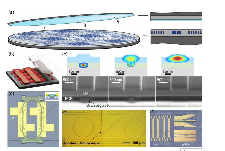
Micro-transfer printing (μTP): Uses a soft PDMS stamp to pick up suspended LN coupons (via tethers or resist supports) and precisely place them on a SiPho target wafer. Offers selective deposition, reduces material waste, supports post-CMOS processing, and enables integration with pre-patterned photonic circuitry (Figures 3–4, pages 6–7). μTP benefits from decoupled source and target wafer processing, allowing LN integration after CMOS back-end steps.
Demonstrators highlighted include:
Mach–Zehnder modulators (MZMs): μTP-enabled single-ended and differential GSSG designs with interaction lengths up to several millimeters achieve Vπ as low as 3.2 V, extinction ratios >30 dB, and EOE bandwidths exceeding 70 GHz (Figure 5, pages 8–9).
Ring modulators and Fabry–Pérot modulators: Compact, energy-efficient devices with selective LN integration, suitable for electro-optic frequency combs and tunable filters.
Nonlinear devices (SHG, Pockels-effect based): Demonstrate the ability of μTP to support advanced photonic functionalities beyond linear modulation.
The review identifies key challenges for μTP: throughput limitations (sequential pick-and-place), alignment precision (achievable ~500 nm 3σ), and limited commercial foundry support. Recent advances, including array printing and centimeter-scale coupon transfers, demonstrate industrial scalability potential.
In conclusion, μTP provides a versatile, selective, and high-precision platform for integrating TFLN onto SiPho, bridging high-performance lithium niobate photonics with industrial-scale photonic integration while enabling modulators, nonlinear devices, and emerging quantum photonic applications.
OMeda (Shanghai Omedasemi Co.,Ltd) was founded in 2021 by 3 doctors with more than 10 years of experience in nanpfabrication. It currently has 15 employees and has rich experience in nanofabrication (coating, lithography, etching, two-photon printing, bonding) and other processes. We support nanofabrication of 4/6/8-inch wafers.