Verification Wafers for Semiconductor Coating Equipment
OMedaSemi provides various verification wafers for semiconductor coating equipment (magnetron sputtering coating equipment, chemical vapor deposition coating equipment, atomic layer deposition coating equipment, electrochemical coating equipment) used in equipment development and process verification.
Type 1: Silicon Trench Wafer
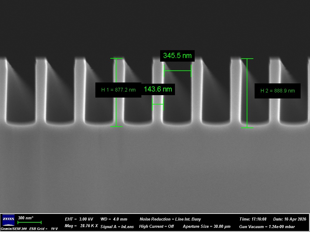
These wafers are primarily used to evaluate the coverage capability of a coating process within deep trenches, determining whether the equipment process can meet the requirements of advanced packaging TSV processes such as deep-hole sputtering.
For large linewidths and deep etching, we use the DRIE BOSCH process; for small linewidths and deep etching, we use the ICP etching process.
Processing capabilities are as follows:
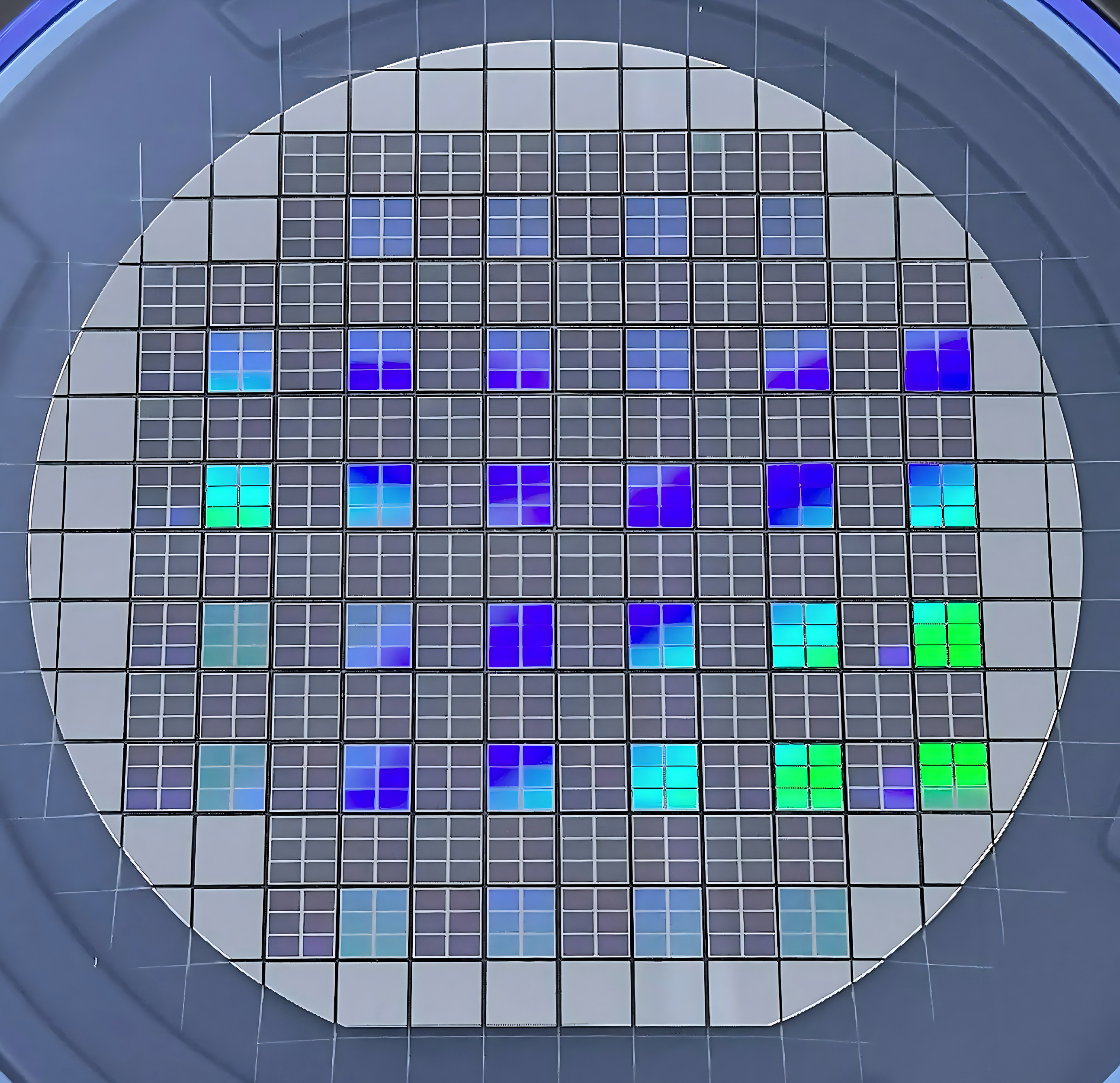
SIZE: 4-12 inches
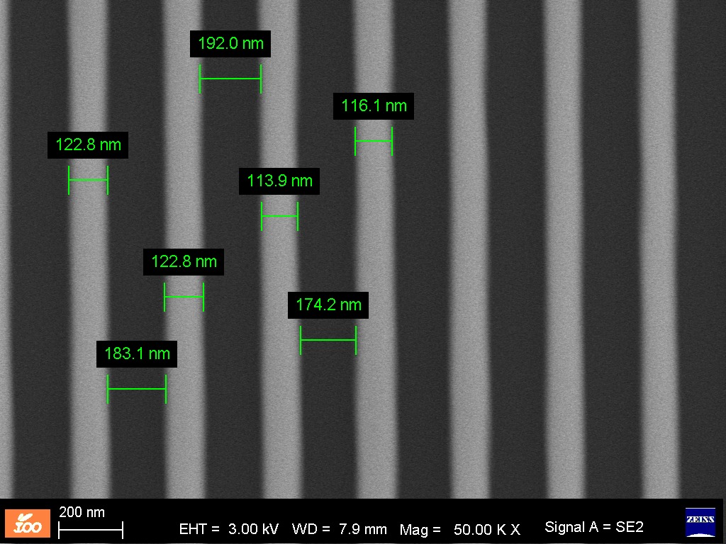
Exposure processes: Electron beam lithography, DUV lithography, contact lithography, laser direct writing
Etching processes and corresponding aspect ratios: DRIE etching (40:1), ICP etching (8:1). The etching aspect ratio is also significantly related to the linewidth.
Etching depth: MAX 1mm @ SIlicon Wafer
Minimum linewidth: 40nm
We have ready-made DUV masks with multiple linewidths:
Hole:
200nm, 400nm, 500nm, 600nm, 1.2um, 2um
Line:
110nm, 200nm, 700nm, 1um, 2um, 4um space
Pillar:
Dia: 150nm, 200nm
Case study: Deep silicon etching trench pattern, CD200nm Etching Depth: 800nm
OMeda (Shanghai Omedasemi Co.,Ltd) was founded in 2021 by 3 doctors with more than 10 years of experience in nanpfabrication. It currently has 15 employees and has rich experience in nanofabrication (coating, lithography, etching, two-photon printing, bonding) and other processes. We support nanofabrication of 4/6/8-inch wafers.