In the processing of aspheric, off-axis aspheric, and freeform surfaces, interferometric detection often relies on compensators or CGH (Computer Generated Hologram) for aberration compensation. However, many engineering sites encounter a seemingly "absurd" phenomenon: the element appears circular, but the test results look flattened; the element appears rectangular, but the result looks trapezoidal. This is not necessarily due to actual deformation in the shape being processed; the more common reason is that the projection distortion (distortion mapping) has not been correctly corrected.
This article reviews from an engineering perspective: where the distortion comes from, why it affects the shaping feedback loop, and the two main distortion correction approaches.
1. Where Does Distortion Come From: Pixel Coordinates ≠ Mirror Coordinates
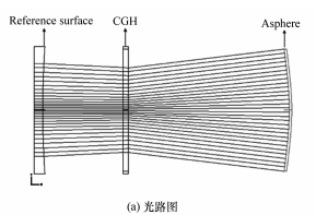
For a sphere, the mapping relationship between the interferometer's output wavefront and the measured surface is relatively simple. However, when the measured surface deviates from the ideal sphere (aspheric/off-axis/freeform surface), to enable the interferometer to "see clearly and accurately," compensators or CGHs must be introduced to transform the interferometer's emitted standard spherical wave into a wavefront that matches the measured surface.
This process leads to a key consequence:
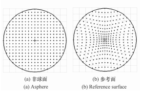
The position of each pixel on the interferometer's image plane no longer maintains a linear correspondence with the lateral positions (x, y) on the mirror surface, but instead forms a complex nonlinear mapping.
In other words, the surface error map provided by the interferometer does not have the same "coordinate system" as the real coordinate system of the component. If the interferometric data is directly used as the real spatial distribution for error judgment or shaping path planning, typical issues such as "shape deformation/boundary distortion/local error misplacement" will occur.
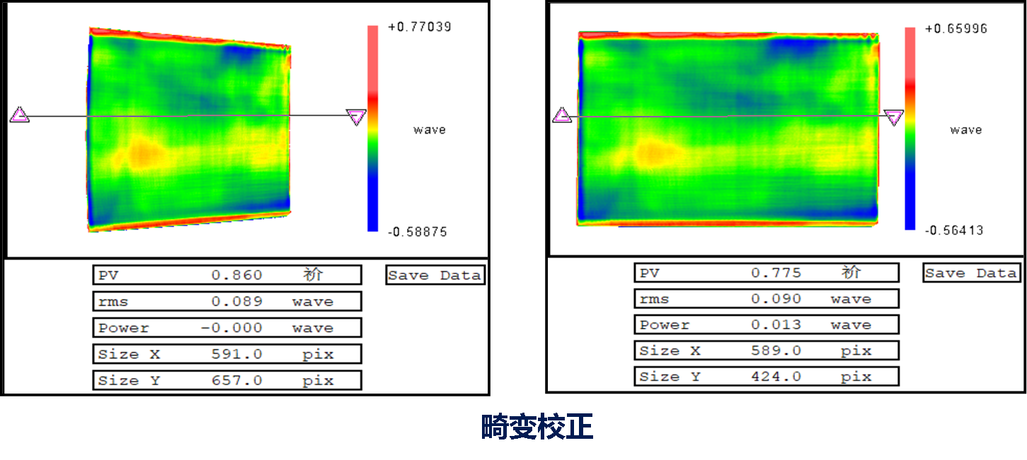
Common manifestations in engineering sites:
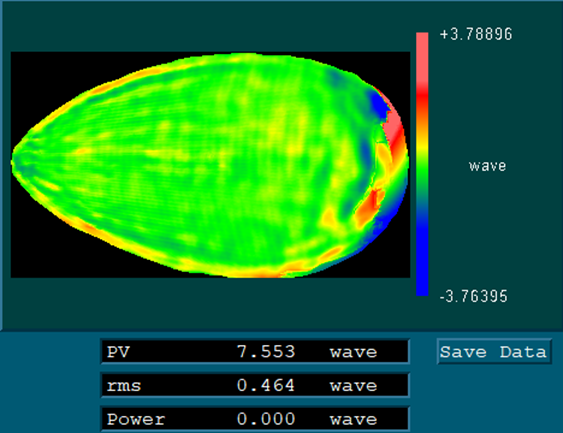
The component is actually circular, but the detection result appears "flattened/elliptical."
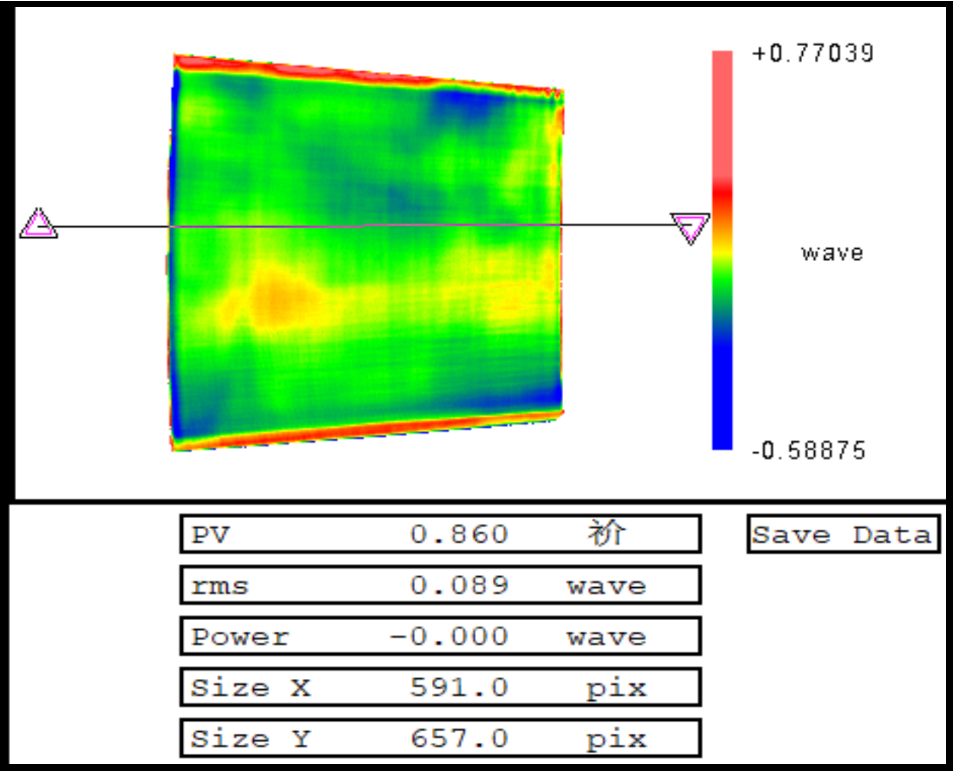
The component is actually rectangular, but the detection result appears "trapezoidal/stretched and skewed."
2. Two Approaches for Distortion Correction: Marker Point Fitting vs Ray Tracing Modeling
The goal of distortion correction is essentially to establish and apply a mapping relationship: interferometer image plane pixel coordinates (u, v) → real coordinates on the measured mirror surface (x, y). Currently, two common approaches are used in engineering.
Approach 1: Marker Point Calibration + Function Fitting (Empirical/Data-Driven)
The method is as follows: a series of identifiable marker points are arranged on the measured mirror surface (or reference plane). The real coordinates (x, y) of the marker points on the mirror are known. These marker points are located in the interferogram to find their corresponding pixel coordinates (u, v), thereby establishing the mapping relationship between pixel coordinates and real coordinates. Polynomial fitting or interpolation methods are then used to fit the nonlinear mapping for the entire image.
Advantages:
The approach is intuitive and has a relatively low implementation threshold. It is suitable for cases with moderate distortion and relatively regular structures.
Pain Points:
The number of marker points is limited by cost, efficiency, and operability. Once the distortion is strong (commonly seen in off-axis/freeform surfaces), a large number of two-dimensional array marker points is often required to "cover" the mapping characteristics. When there are insufficient points, fitting will result in local distortions, leading to position errors even after correction.
Approach 2: Ray Tracing Based on System Model (Physics/Model-Driven)
Another approach is to start from the measurement system itself: model and trace rays through the entire optical path of the "interferometer—compensator/CGH—measured mirror surface" to directly calculate the coordinates on the mirror surface corresponding to the pixel coordinates (or field angle/ray bundles) on the image plane. This enables the precise "re-mapping" of the height error data measured by the interferometer into the real mirror coordinate system.
Advantages:
More robust for complex distortions, especially suitable for off-axis aspheric and freeform surfaces. It has stronger physical consistency and is easier to form a reusable engineering process (different components/different optical paths can be configured).
Key Requirements:
The optical model parameters must be accurate (component posture, spacing, surface shape, CGH parameters, etc.).
Mature software implementation and engineering validation are required (otherwise, the correctness of the model is hard to guarantee).
3. How to Determine if You "Must Do Distortion Correction"
If any of the following signals appear, it is recommended to treat distortion correction as a mandatory step, rather than an "optional optimization":
The boundary shape of the detection result clearly deviates from the actual aperture (circle becomes flattened, rectangle becomes trapezoidal, etc.).
After shaping, the error does not converge, or "the more you correct, the messier it gets," with hotspot positions not aligning.
As the off-axis amount increases, the error map shows obvious stretching, tilting, or local squeezing.
If you are implementing CGH detection in an engineering application, distortion correction is often a critical step that transitions from "being measurable" to "being correctable and having a closed-loop."
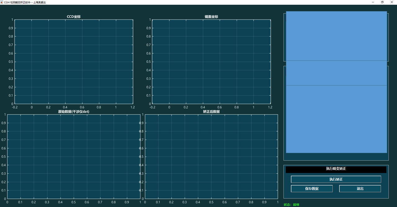
The distortion correction software developed by Shanghai Omida covers distortion correction for all optical paths, including traditional compensators, off-axis parabolic self-collimation methods, and CGH detection! Below is a software schematic. If you have other software needs, please contact Shanghai Omida! For high-precision CGH design and manufacturing, please contact Shanghai Omida at https://www.omedasemi.com