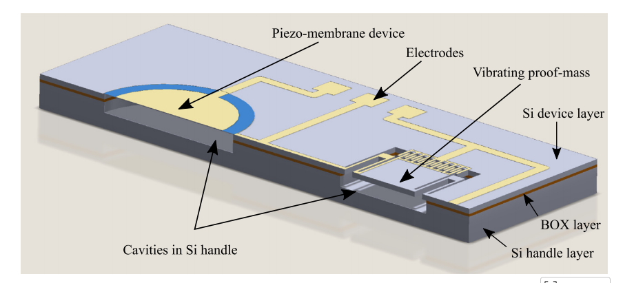
The article presents a novel method for aligning patterns on thick device layers to cavity patterns in the handle layers of pre-fabricated cavity-SOI (c-SOI) wafers, aimed at improving MEMS (Micro-Electro-Mechanical Systems) production. The method uses a standard ASML PAS5500 wafer stepper and does not require specialized lithography or alignment equipment, making it accessible and cost-effective for MEMS fabrication.
Key points:
The method involves positioning alignment markers at the wafer edge of the handle layer and utilizing a "terracing" process to expose these markers after wafer bonding. This is beneficial for detecting and aligning markers for lithography.
The process showed successful detection of alignment markers on wafers with different device layer thicknesses (simulated using polymeric layers of 30 μm and 80 μm).
The study quantified the offset in alignment due to out-of-plane alignment and image projection, finding that offsets increased from < 25 nm for control wafers to < 160 nm for wafers with 80 μm thick device layers. However, these offsets are small enough for most MEMS applications.
The results suggest two methods for further reducing these offsets: correcting image projections with average offsets based on radial position, or storing offset values in a per-wafer database for future corrections.
The study concludes that this alignment process is feasible using standard cleanroom equipment, offering performance comparable to state-of-the-art wafer bonding systems. It provides a practical solution for integrating c-SOI technology into advanced MEMS applications, with potential for highly integrated, cost-effective microdevices in areas such as biomedical systems.
OMeda (Shanghai Omedasemi Co.,Ltd) was founded in 2021 by 3 doctors with more than 10 years of experience in nanpfabrication. It currently has 15 employees and has rich experience in nanofabrication (coating, lithography, etching, two-photon printing, bonding) and other processes. We support nanofabrication of 4/6/8-inch wafers.