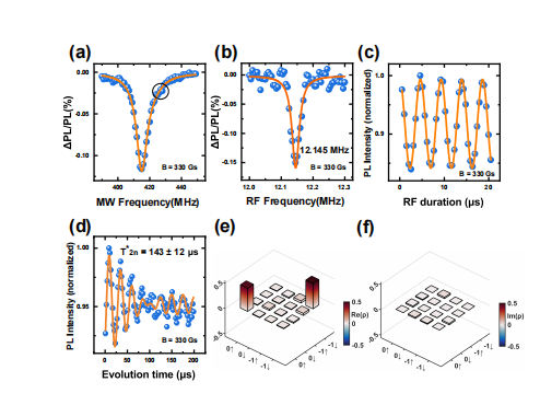
The article explores the creation of a fully functional quantum node using silicon carbide (SiC), where a PL6 color center’s electron spins act as the processor qubit and nearby nuclear spins serve as memory qubits. The main innovation lies in the design of a pulse sequence that combines dynamical decoupling and radiofrequency (RF) control, enabling decoherence-protected universal gate operations between processor and memory qubits. This method preserves coherence, ensuring high-fidelity quantum operations. The node demonstrated the ability to prepare and manipulate entangled states with a fidelity of 90 ± 3%, surpassing the fault-tolerance threshold required for certain quantum network architectures.
Key aspects of the article include:
Quantum Node Architecture: The node uses a hybrid system of electron and nuclear spins, where the electron spin provides fast control as the processor, and the nuclear spin functions as a long-lived memory qubit.
Decoherence-Protected Gate Operations: A composite pulse sequence was implemented that combines microwave and RF pulses, which enables universal gate operations while protecting the system from decoherence, a key challenge in maintaining quantum coherence.
Entanglement and Fidelity: The system can create entangled states between processor and memory qubits, with a fidelity of 90 ± 3%, making it suitable for scalable quantum network applications.
Performance of the Quantum Node: The article highlights how the entangling gate operations were successfully implemented, demonstrating that the node could function reliably even when subjected to realistic experimental conditions.
This work provides a promising approach for scalable quantum networks, leveraging SiC's unique material properties and established semiconductor technologies to construct robust quantum nodes. The results pave the way for advancements in quantum communication, computing, and sensing by offering a method to overcome the challenges of coherence preservation and entanglement generation in solid-state systems.
OMeda (Shanghai Omedasemi Co.,Ltd) was founded in 2021 by 3 doctors with more than 10 years of experience in nanpfabrication. It currently has 15 employees and has rich experience in nanofabrication (coating, lithography, etching, two-photon printing, bonding) and other processes. We support nanofabrication of 4/6/8-inch wafers.