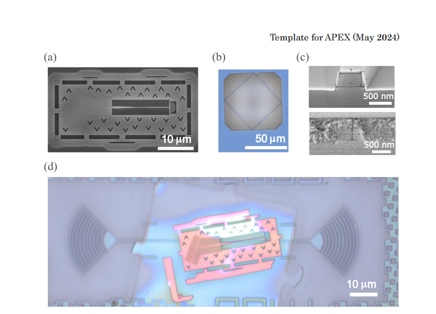
The article presents the hybrid integration of an InAs/GaAs quantum dot (QD) single-photon source (SPS) with a silicon nitride (SiN) photonic integrated circuit using a coupled crossover waveguide structure. The primary challenge of efficiently coupling the QD emission from GaAs to SiN is addressed through a unique structure that utilizes a photonic crystal nanocavity for funneling QD emission into a GaAs waveguide, which then transfers photons to a SiN waveguide at the crossover section via evanescent coupling. This integration enables the creation of a high-efficiency single-photon source on a SiN photonic platform.
Key findings from the study include:
Hybrid Integration Approach: The InAs/GaAs QD is integrated into a SiN circuit using a coupled crossover waveguide structure, significantly improving coupling efficiency between GaAs and SiN despite their large refractive index mismatch.
Purcell Enhancement: The QD emission undergoes Purcell enhancement through coupling with a photonic crystal nanocavity, resulting in increased single-photon emission efficiency.
High Coupling Efficiency: The design supports over 90% coupling efficiency from the QD emission into the SiN waveguide, with the experimentally observed coupling efficiency reaching 91.8%.
Experimental Results: The system demonstrated successful on-chip photon propagation and outcoupling through a SiN grating coupler. Time-resolved measurements revealed a Purcell factor of 3.3, indicating efficient coupling and enhanced emission rates.
Quantum Nature of Emission: Intensity correlation measurements confirmed the quantum nature of the QD emission, with a measured second-order correlation function g(2)(0) of 0.34 after background correction, indicating low background noise and high purity.
The article concludes that the coupled crossover waveguide structure overcomes the limitations of traditional integration techniques for GaAs and SiN systems. The demonstrated hybrid integration scheme opens the door for scalable quantum photonic systems that can be integrated with existing semiconductor technology, offering significant potential for future quantum communication and information processing applications.