The document you uploaded discusses single-photon emitters and spin-photon interfaces in silicon, focusing on their applications in quantum computing, quantum networks, and photonic quantum information processing. Here’s a summary of the key points from the article:
Introduction to Single-Photon Emitters and Spin-Photon Interfaces: The document starts by explaining the importance of single-photon emitters in quantum technology. It highlights that silicon-based systems are increasingly being considered for these purposes due to their scalability, the high purity of silicon, and the potential for long spin coherence times. These properties make silicon an attractive material for building quantum nodes and enabling quantum communication and networking.
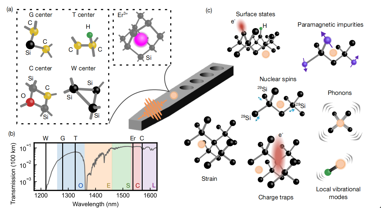
Types of Emitters: The document distinguishes between two primary types of emitters in silicon: dopant atoms (such as erbium) and color centers. These emitters can facilitate the generation of single photons, with some systems also enabling spin-photon interfaces that can store quantum information for extended periods. It also discusses the different types of color centers, such as T, G, W, and C centers, and their respective properties.
Challenges and Solutions: One of the major challenges in implementing efficient single-photon sources and spin-photon interfaces is ensuring spectral stability and coherence. The document describes how nanophotonic structures can be used to overcome some of these limitations by enhancing light extraction efficiency and shortening the emitter's lifetime. This helps maintain photon coherence while improving emitter performance.
Integration into Nanophotonic Structures: The document outlines the use of silicon nanophotonic devices, including waveguides and optical resonators, to improve photon extraction and emitter integration. These devices help in confining light and ensuring that the emitted photons are collected efficiently. This also helps in overcoming issues such as non-radiative decay and fluctuating transition frequencies that can affect the quality of photon emission.
Applications and Scalability: The document emphasizes the potential for scaling up silicon-based quantum devices. It explores how integrating single-photon emitters and spin-photon interfaces into larger systems could lead to advancements in quantum sensing, communication, and distributed quantum computing. The document also discusses the challenges involved in upscaling, such as achieving high-fidelity photon emission and integrating these devices with existing fiber-optic infrastructure.
Summary and Outlook: The review concludes with an optimistic outlook on the future of silicon-based single-photon emitters and spin-photon interfaces. It highlights the progress in materials and device fabrication that could lead to more efficient and scalable systems for quantum applications. The article suggests that continued advancements in material science and quantum computing will likely lead to the development of high-quality, scalable quantum devices using silicon.
This review highlights the promising future of silicon as a key platform for quantum technologies, particularly in the context of scalable single-photon sources and spin-photon interfaces.
OMeda (Shanghai Omedasemi Co.,Ltd) was founded in 2021 by 3 doctors with more than 10 years of experience in nanpfabrication. It currently has 15 employees and has rich experience in nanofabrication (coating, lithography, etching, two-photon printing, bonding) and other processes. We support nanofabrication of 4/6/8-inch wafers.