This article presents the development and application of a new advanced substrate, cavity-BOX SOI, designed for the fabrication of microelectromechanical systems (MEMS). The key feature of the cavity-BOX substrate is its pre-patterned buried oxide (BOX) layer, which provides significant advantages in MEMS device fabrication, such as greater design freedom and simplified processes.
The cavity-BOX substrate is created by patterning cavities in the BOX layer of a silicon-on-insulator (SOI) wafer, allowing for precise alignment of the device layer structures. This technique overcomes limitations in traditional cavity-SOI substrates, such as restricted cavity size and alignment precision, by offering almost unlimited design flexibility for cavity dimensions and maintaining the mechanical integrity of the wafer.
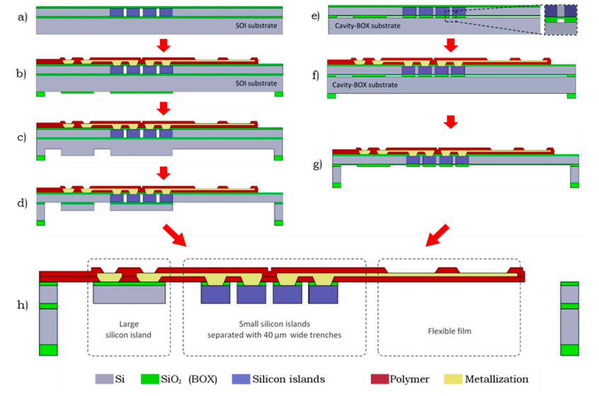
A practical application of the cavity-BOX substrate is demonstrated in the fabrication of a Deep Brain Stimulation (DBS) demonstrator. The device features small silicon islands and a flexible polymer film, designed to be semiflexible and compact. The cavity-BOX substrate enables a simplified process for creating the device's complex geometries, such as high-precision micron-sized structures and large openings for integration with electronic components like ASICs (application-specific integrated circuits).
The paper highlights the advantages of using cavity-BOX substrates, including reduced etching complexity, improved precision, and greater flexibility in MEMS designs. The fabricated DBS device, with dimensions of 18 mm length and 1.2 mm diameter, demonstrates the robustness and efficiency of the cavity-BOX process, making it suitable for scalable production of MEMS devices that require precise feature definition and thin device layers.
The study also discusses challenges in the fabrication process, including issues with alignment accuracy and terrace width, which affect compatibility with standard cleanroom equipment. Despite these challenges, the cavity-BOX approach is shown to significantly improve the fabrication process, offering a more robust, scalable, and efficient solution for MEMS and flexible devices.
OMeda (Shanghai Omedasemi Co.,Ltd) was founded in 2021 by 3 doctors with more than 10 years of experience in nanpfabrication. It currently has 15 employees and has rich experience in nanofabrication (coating, lithography, etching, two-photon printing, bonding) and other processes. We support nanofabrication of 4/6/8-inch wafers.