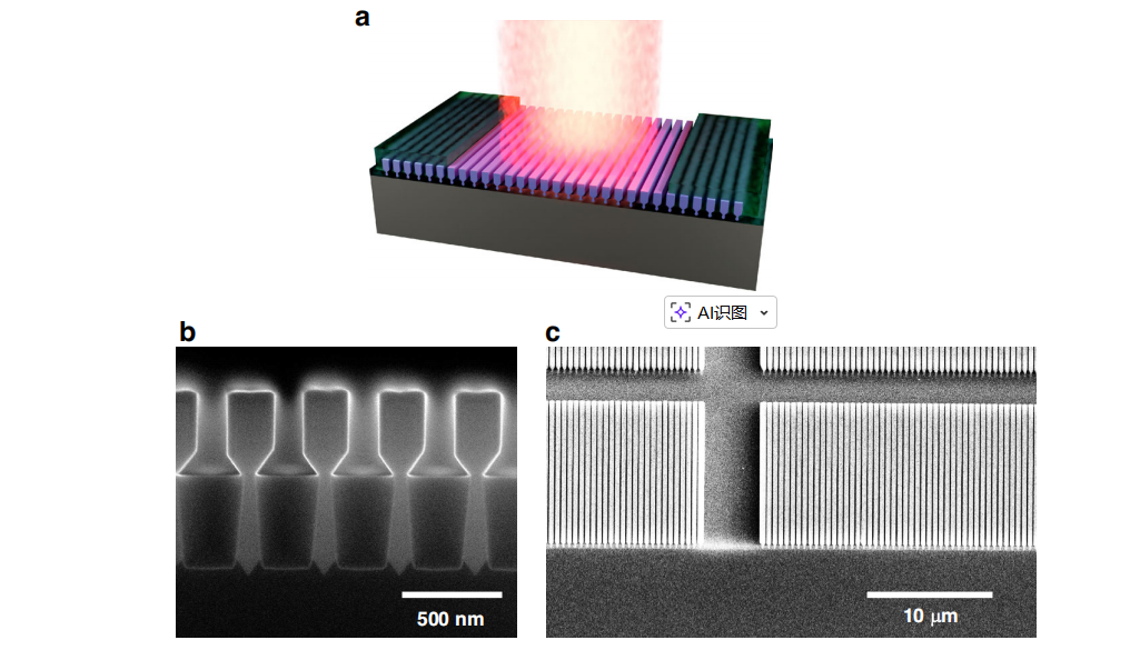
This study reports the first experimental demonstration of surface-emitting nano-ridge lasers (NRSELs) epitaxially grown on standard 300 mm silicon wafers. Using aspect ratio trapping (ART) and nano-ridge engineering (NRE), high-quality InGaAs/GaAs nano-ridges with embedded quantum wells are grown directly on silicon, achieving low defect densities and eliminating the need for thick buffer layers. The nano-ridge arrays form a one-dimensional photonic crystal, supporting band-edge quasi-TE modes and symmetry-protected bound states in the continuum (BICs), enabling high-Q lasing and vertical light emission without traditional thick DBR mirrors.
The study combines FDTD simulations and experimental measurements to optimize nano-ridge dimensions, array periodicity, and cavity design. A combination of side mirrors formed from photoresist and careful cavity engineering suppresses in-plane losses, increasing the Q-factor from 15,000 to 26,000 for a 40-period device. Micro-photoluminescence measurements reveal low lasing thresholds (~5–10 kW/cm²), single-mode operation, narrow linewidths (~0.9 nm), and tunable emission across ~980–1060 nm by adjusting the nano-ridge width and height. Back-focal-plane imaging confirms tight angular confinement (<10°) and demonstrates star-shaped emission patterns corresponding to the band-edge modes.
The NRSEL platform offers scalable, CMOS-compatible integration of vertically emitting lasers on silicon, with potential for multi-wavelength arrays, electrically injected operation, and flexible spectral coverage by modifying material composition (e.g., InGaAs or GaSb). These results suggest broad applicability in silicon photonics, telecommunications, LIDAR, environmental sensing, and spectroscopy, overcoming key limitations of conventional VCSELs such as restricted wavelength range and complex epitaxial growth
OMeda (Shanghai Omedasemi Co.,Ltd) was founded in 2021 by 3 doctors with more than 10 years of experience in nanpfabrication. It currently has 15 employees and has rich experience in nanofabrication (coating, lithography, etching, two-photon printing, bonding) and other processes. We support nanofabrication of 4/6/8-inch wafers.