This work reports a high-frequency thin-film lithium niobate (LiNbO₃) acoustic resonator achieving 50.74 GHz operation with a quality factor (Q) of 237 and electromechanical coupling (k²) of 5.17%, resulting in a figure of merit (FoM = Q·k²) of 12.2. The device also exhibits an S2 mode at 16.99 GHz with Q = 159, k² = 65.06%, and FoM = 103.4, demonstrating the potential for wideband millimeter-wave (mm-wave) front-end applications.
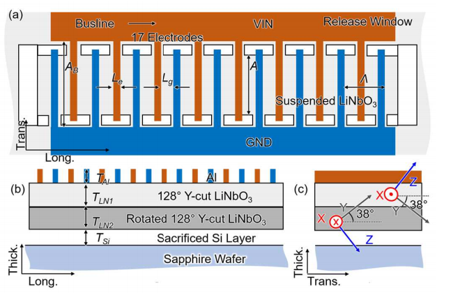
The resonator uses a bilayer periodically poled piezoelectric film (P3F) structure composed of two 128° Y-cut LiNbO₃ layers bonded on amorphous silicon (a-Si) on sapphire. By utilizing higher-order symmetric bulk acoustic modes (S2 and S6), the design maintains strong coupling and high Q while allowing larger lateral feature sizes and thicker films, overcoming challenges associated with scaling conventional thin-film devices to mm-wave frequencies (pages 1–2).
Design and simulation using COMSOL finite element analysis show well-confined acoustic modes with k² = 58.2% at 16.1 GHz (S2) and 7.7% at 50.26 GHz (S6). Fabrication involves photolithographic etching of the LiNbO₃ layers, e-beam deposition of 350 nm Al electrodes, and XeF₂ release for mechanical isolation (page 2). TEM imaging confirms bilayer thicknesses of ~105 nm and 80 nm, with slight variation across the wafer (page 2).
Experimental results using a modified Butterworth Van-Dyke model reveal state-of-the-art performance, surpassing prior works at corresponding frequencies. The high Q and k² are attributed to the bilayer P3F structure, sacrificial a-Si layer, and sapphire substrate, which reduce mechanical losses and support high-order modes (page 3–4).
In conclusion, the study demonstrates record-breaking mm-wave acoustic resonators with a high figure of merit, validating the bilayer P3F LiNbO₃ platform as a promising candidate for compact mm-wave filters and other high-frequency front-end components .
OMeda (Shanghai Omedasemi Co.,Ltd) was founded in 2021 by 3 doctors with more than 10 years of experience in nanpfabrication. It currently has 15 employees and has rich experience in nanofabrication (coating, lithography, etching, two-photon printing, bonding) and other processes. We support nanofabrication of 4/6/8-inch wafers.