Paper Download
 Copper Damascene Process-Based High-Performance Thin Film Lithium Tantalate Modulators.pdf
OMedaSemi can provide 4-inch and 8-inch LNOI wafers and LN-SOI
We provide 4-8 inch LNOI wafers (thin-film lithium niobate), which use surface activated bonding or Hydropholic bonding(Directly Bonding) technology to bond thermal oxide wafers and Lithium niobate crystal(Xcut and Zcut)(Congrudent LN ,Stochoimetric LN,MgO:Doped LN) wafers together, and then control the thickness to the thickness you need through ion implantation, annealing, thinning(Thin Fiim LN<600nm) or="" direct="" thinning="" and="" cmp="" thick="" fiim="" ln="">600nm) . It is worth noting that ion implantation and direct CMP and thinning have their own advantages and disadvantages. We provide customers with a variety of LNOI products. Also we have 6inch LTOI(lithium tantalate) wafer and PZTOI Wafer (A Novel Electro-Optical Platform).
To learn more, please click the following link:https://en.omedasemi.com/linbo3_on_insulator.html
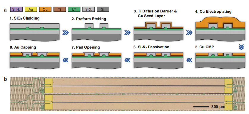
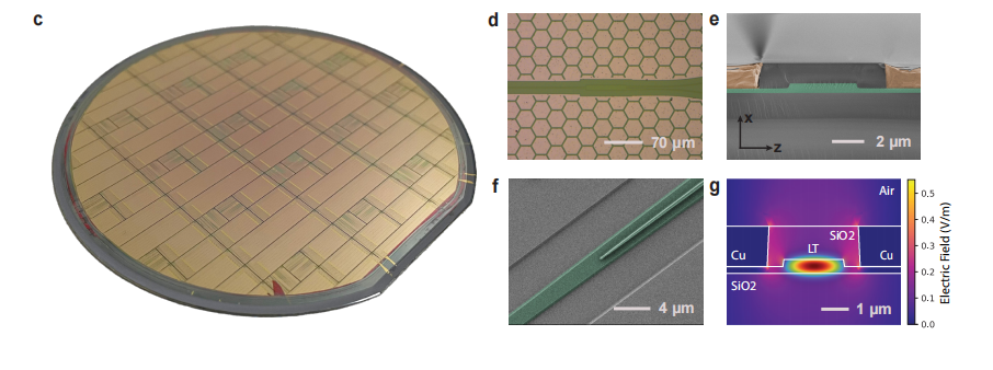
The article presents a significant advancement in the fabrication of electro-optic (EO) modulators, specifically focusing on a new copper Damascene process for creating high-performance thin-film lithium tantalate (TFLT) modulators. These devices are critical for modern optical communication systems, which need efficient interfaces between electrical and optical signals.
The copper Damascene process improves the performance of TFLT-based modulators by providing low-loss microwave electrodes, essential for reducing signal losses. The copper electrodes outperform traditional gold ones, achieving a 10% reduction in microwave losses. Additionally, this process allows the modulators to be integrated more effectively with microelectronics through chip-on-wafer bonding, a technique commonly used in modern electronics.
The article demonstrates the capabilities of these modulators in high-speed data transmission, with results showing data rates up to 540 Gbit/s in PAM8 schemes, and reaching a maximum net data rate of 423 Gbit/s. The modulators also maintain a low bit error rate, making them suitable for high-capacity communication systems.
This work opens the door for scalable manufacturing of integrated electro-optic devices, pushing forward the integration of optical modulators with microelectronic circuits, and thus paving the way for next-generation photonic systems used in data communications and artificial intelligence applications.
OMeda (Shanghai Omedasemi Co.,Ltd) was founded in 2021 by 3 doctors with more than 10 years of experience in nanpfabrication. It currently has 15 employees and has rich experience in nanofabrication (coating, lithography, etching, two-photon printing, bonding) and other processes. We support nanofabrication of 4/6/8-inch wafers.