Paper Download
 Integrated Electro-Optics on Thin-Film Lithium Niobate.pdf
We provide 4-6 inch LTOI wafers (thin film lithium tantalate),We can provide 4inch 6inch 8inch(on developing) lithium tantalate on insulator wafer , Both thin film (300-600nm) by smartcut process and Thick Film (>600nm) by Grinding+CMP process
To learn more, please click the following link:https://en.omedasemi.com/litao3_on_insulator.html
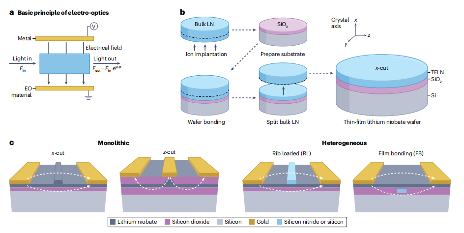
The article provides a comprehensive review of integrated electro-optics using thin-film lithium niobate (TFLN), highlighting the technology's potential and advancements in electro-optic (EO) modulation. The paper discusses the fundamental principles of electro-optic modulation, focusing on the unique properties of TFLN, such as strong EO interaction, low optical loss, high microwave bandwidth, and scalable reconfigurability. These attributes enable the development of high-performance devices for various applications, including communications, quantum optics, and sensing.
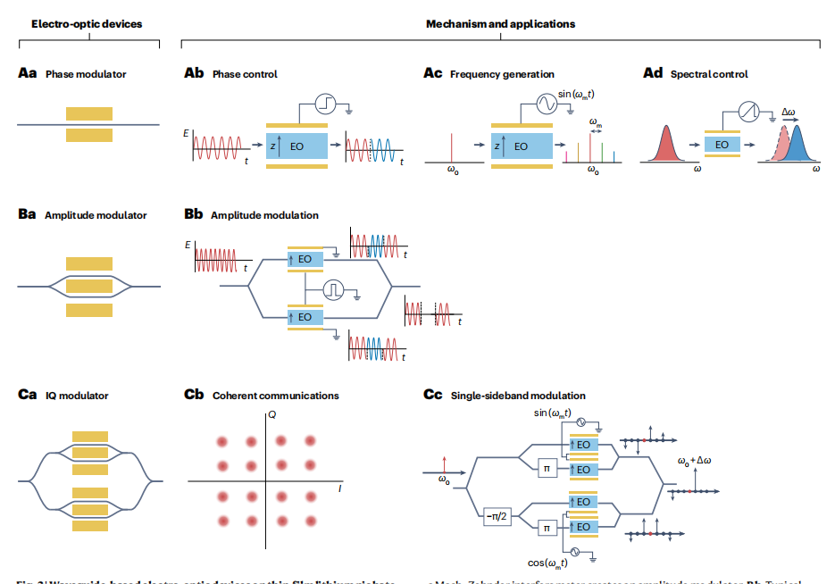
The review covers recent developments in TFLN-based electro-optic devices, particularly the improvements in modulators, resonators, and coupled-cavity devices. TFLN's ability to integrate nonlinear optical effects and its compatibility with existing nanofabrication techniques make it a promising platform for exploring complex physical phenomena and creating innovative photonic devices.
Emerging applications of TFLN integrated electro-optics include frequency comb generation, quantum electro-optics, and the development of new functionalities that were previously unattainable in bulk systems. The paper also explores the challenges of large-scale TFLN fabrication, highlighting efforts in heterogeneous integration with silicon and silicon nitride for enhanced performance and scalability.
Overall, TFLN is presented as a transformative platform for next-generation electro-optic devices, enabling advanced photonic systems that bridge the gap between electronics and photonics for high-speed, energy-efficient, and scalable applications.
OMeda (Shanghai Omedasemi Co.,Ltd) was founded in 2021 by 3 doctors with more than 10 years of experience in nanpfabrication. It currently has 15 employees and has rich experience in nanofabrication (coating, lithography, etching, two-photon printing, bonding) and other processes. We support nanofabrication of 4/6/8-inch wafers.