
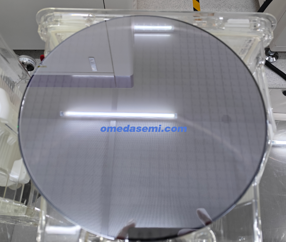
OMedaSemi offers 12 inch BUMP wafer processing, and we also have standard BUMP wafers available for sale for equipment manufacturers to use for equipment calibration and validation.
Business Model:
Customers who come to us for Bump wafer processing generally fall into two categories:
Type 1: Bump wafers processed using our existing masks, used for semiconductor metrology/inspection testing or semiconductor process equipment debugging. For such customers, we charge a one-time per-wafer fee, with no other additional charges.
Type 2: For such customers, we charge a MASK (reticle) fee, an NRE process development fee, and a per-wafer production processing fee.
Capbility:
Bump Type:Solder Bump/Pillar Bump
Bump Structure:CuNiSnAg、CuSnAg、 NiAu
Min. Bump Size:12um
Min. Bump Pitch:22um
Min. Solder Ball Size:150um
Min. Solder Ball Pitch:250um
Dicing Services: Blade dicing, laser stealth dicing, plasma dicing
Processing Cycle Time:
Type 1 customers: 2 weeks
Type 2 customers: 2-3 weeks
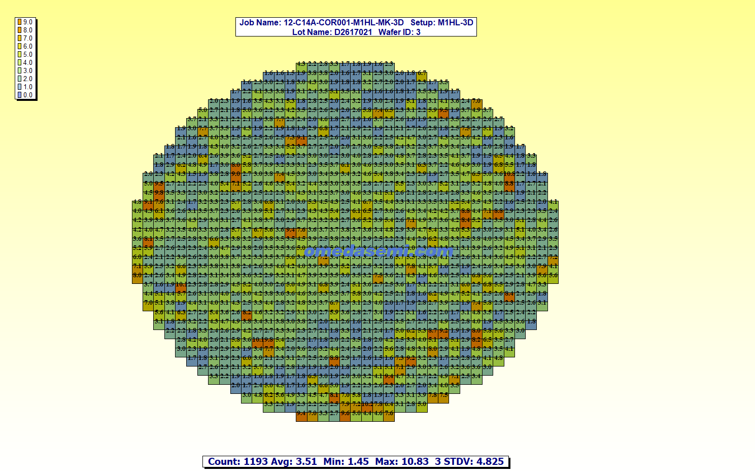
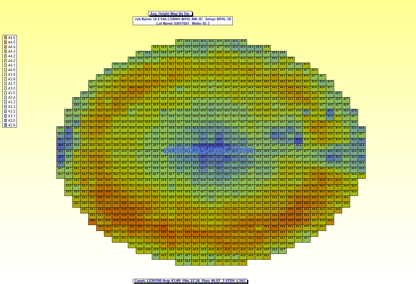
Testing: After processing is completed, we provide coplanarity data for all bumps within a single chip and height data for all bumps within a single chip.

OMeda (Shanghai Omedasemi Co.,Ltd) was founded in 2021 by 3 doctors with more than 10 years of experience in nanpfabrication. It currently has 15 employees and has rich experience in nanofabrication (coating, lithography, etching, two-photon printing, bonding) and other processes. We support nanofabrication of 4/6/8-inch wafers.
