The study investigates the dispersion characteristics of surface phonon polaritons (SPhPs) in free-standing silicon carbide (SiC) thin films of 100 nm and 200 nm thickness. SPhPs are hybrid light–matter excitations that couple photons with optical phonons, enabling subwavelength confinement and strong field enhancement in polar dielectrics. The authors utilize scattering-type scanning near-field optical microscopy (s-SNOM) combined with nano-FTIR spectroscopy to probe the SPhP modes at nanoscale spatial resolution.
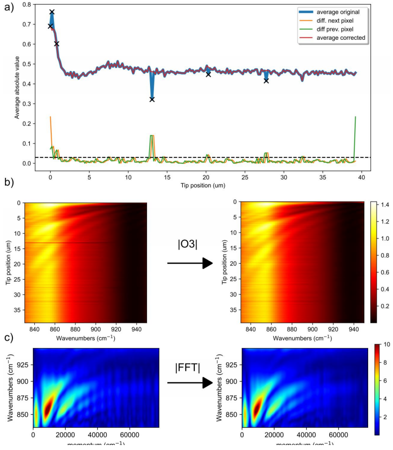
Key contributions include the development of data processing pipelines to isolate edge-launched polariton modes, remove baseline artifacts, and extract the dispersion relation from complex-valued amplitude and phase maps. Advanced procedures, including Fourier analysis, inverse FFT, and windowing, are applied to recover the polariton wavevector and propagation lengths accurately. The study also employs patterned chromium strips on the membranes to enhance SPhP launching efficiency and to facilitate nano-imaging of the modes.
Experimental results demonstrate good agreement with theoretical models. Edge-launched SPhPs exhibit propagation lengths of several tens of microns, and lifetimes of approximately 7.9 ps for 200 nm membranes and 9.7 ps for 100 nm membranes. Angle-dependent measurements confirm the predicted orientation dependence of the dispersion, while substrate-supported SiC films show significantly reduced excitation efficiency due to redshifted modes. The work provides a robust methodology for quantitative near-field mapping of SPhPs, offering insights relevant for nanoscale photonics, thermal management, and polaritonic device design.
OMeda (Shanghai Omedasemi Co.,Ltd) was founded in 2021 by 3 doctors with more than 10 years of experience in nanpfabrication. It currently has 15 employees and has rich experience in nanofabrication (coating, lithography, etching, two-photon printing, bonding) and other processes. We support nanofabrication of 4/6/8-inch wafers.