
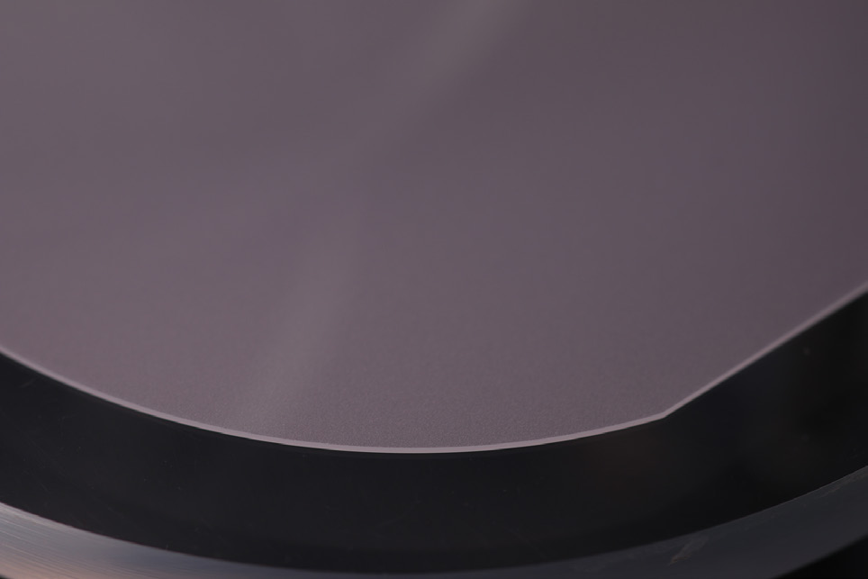
OMedaSemi can provide customers with high-quality standard sapphire-based aluminum nitride templates in 2/4/6-inch sizes, with aluminum nitride film thicknesses ranging from 200-1000nm. We can also customize non-standard sapphire-based aluminum nitride templates in corresponding sizes and film thicknesses from 50-5000nm. Our products are widely used in UV-LED chips, ultraviolet detectors, and other fields.
| Specifications | paameter value | ||||
| ProductNumber | UTI-AIN-050A | UTI-AIN-100A | UTI-AIN-150A | ||
| substrate | Sapphire C-side | ||||
| AIN epitaxial layer cystal structure | Wurtzite | ||||
| Diameter(inches) | 2 | 4 | 6 | ||
| Substrate thickmess(m) | 430±15 | 650±20 | 1300±20 | ||
| AIN epitaxial layer thickmes5(nm) | 200/400/600/800/1000 or customized.The parameters in this table are based on 200mm as am example | ||||
| Crystal orientation | C-axis [0001]+/-0.2° | ||||
| crack | nothing | ||||
| Back roughness(m) | RMS<1.2 | ||||
| HRXRD half width @(0002)(arcsec) | <100 | ||||
| HRXRD half width@(10-12)(arcsec) | <350 | ||||
| Surface roughnes5[5×5um](nm) | Ra≤2 | ||||
| Total thickmess variation(m) | ≤10 | ≤20 | ≤20 | ||
| Warping degree(m) | ≤20 | ≤40 | ≤60 | ||
| Bending degree(m) | ≤20 | ≤40 | ≤60 | ||
| Packaging | Single wafer round box/Multi wafer round box | ||||
Sapphire-based aluminum nitride thin film template: Partial characterization results (200 nm as an example)
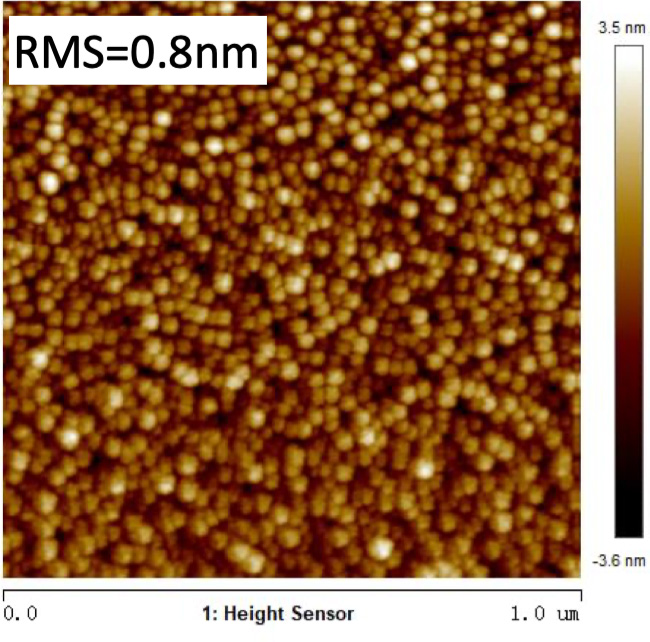
FIg1:Roughness of ALN EPI
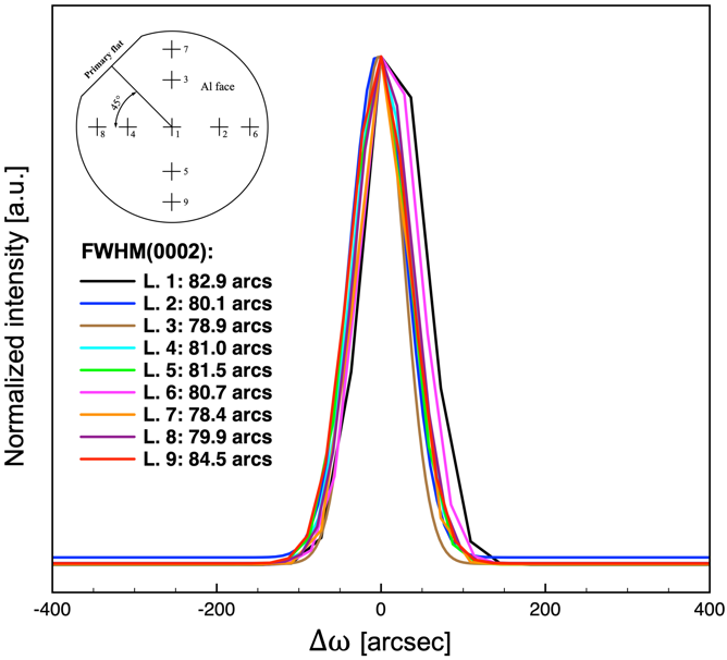
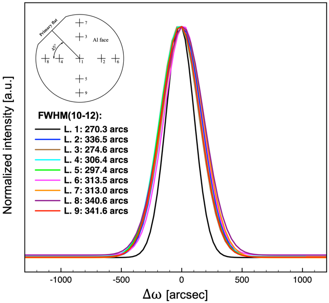
FIG2:Sapphire-based AlN thin film template 002/102 HRXRD half-width
OMeda (Shanghai Omedasemi Co.,Ltd) was founded in 2021 by 3 doctors with more than 10 years of experience in nanpfabrication. It currently has 15 employees and has rich experience in nanofabrication (coating, lithography, etching, two-photon printing, bonding) and other processes. We support nanofabrication of 4/6/8-inch wafers.
