
OMedaSemi provide thermal oxide wafer for photonics application
For Silicon Photonics:
generally 2um 3um
For Silicon Nitride:
generally 3um 8um 10um 15um
For LNOI and LTOI :
2um 4.7um 7um 8um 10um 15um
Case 1:
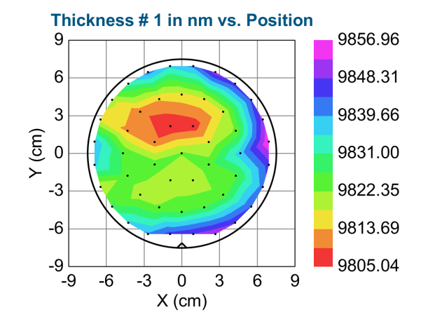
6inch 10um thermal oxide wafer
Uniformity :0.56%
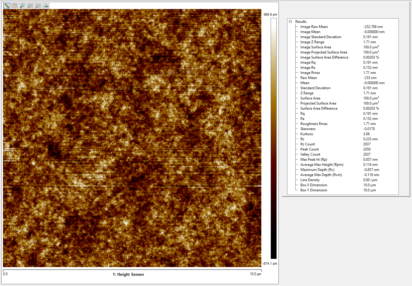
Roughness:Ra=0.152nm
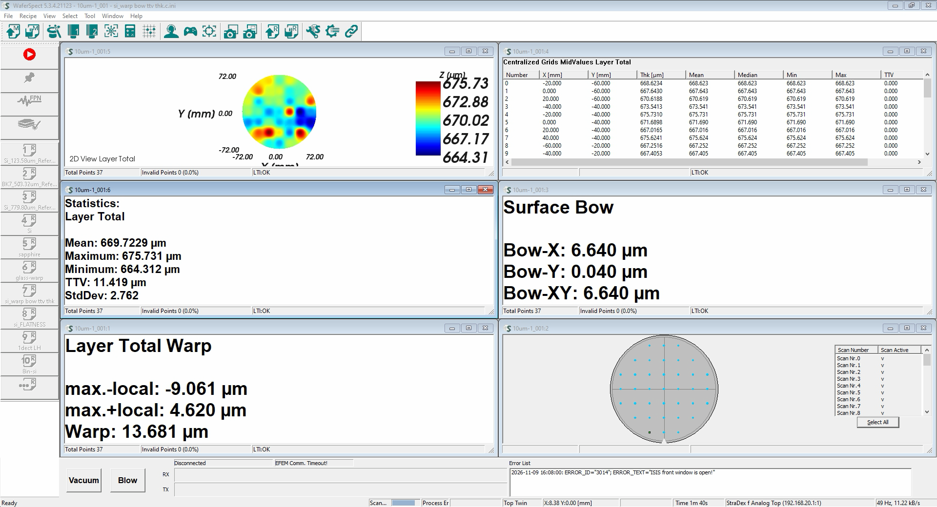
TTV:11.419um(it could be better if we use better silicon substrate )
Bow:6.64um
warp:13.681um
OMeda (Shanghai Omedasemi Co.,Ltd) was founded in 2021 by 3 doctors with more than 10 years of experience in nanpfabrication. It currently has 15 employees and has rich experience in nanofabrication (coating, lithography, etching, two-photon printing, bonding) and other processes. We support nanofabrication of 4/6/8-inch wafers.
