
OMedaSemi provides DBR coating technology services.
Supported high and low refractive index material systems: (contact sales for refractive index data)
- SiO2-TiO2
- SiO2-Ta2O5
- SiO2-HfO2
Supported coating methods:
Ion Beam Assisted Electron Beam Evaporation Coating:
- Coating temperature: 150-200°C
- Equipment capacity: 20 pcs of 4-inch wafers, 5 pcs of 6-inch wafers
Magnetron Sputtering Coating:
- Coating temperature: <100°C
- Equipment capacity: 4 pcs of 6-inch wafers
Ion Beam Sputtering Coating:
- Coating temperature: 150-200°C
- Equipment capacity: 4 pcs of 6-inch wafers
Supported substrates: Silicon, glass, silicon carbide, substrates with photoresist, and other substrates, etc.
Post-coating dicing services are also supported.
Business Model:
Customers who come to us for DBR coating technology services generally fall into two categories:
Type 1: We provide refractive index data, and Party A designs the material film stack. We perform the coating process according to Party A's film layers, and ultimately do not guarantee the result. If needed, we can assist in testing the transmittance and reflectance data of the film layer using a spectrophotometer.
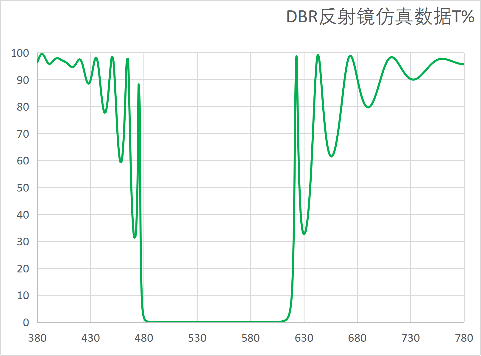
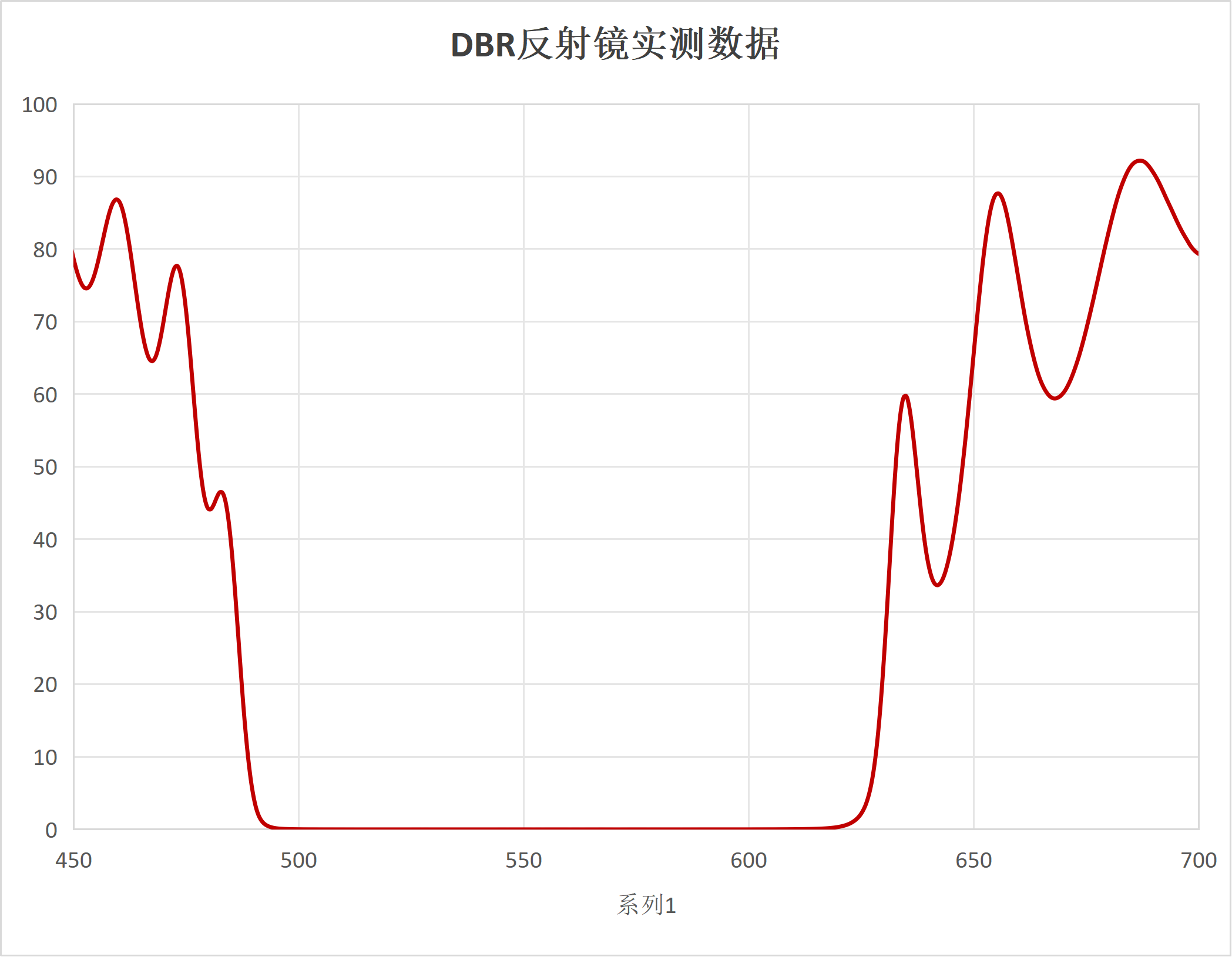
Type 2: Party A provides optical requirements, such as transmittance and reflectance data for a certain wavelength band. We design the film stack according to Party A's optical requirements, provide film stack simulation data, and optical simulation transmittance and reflectance data to Party A for confirmation. After confirmation, Party B performs the processing. After processing is completed, Party B uses a spectrophotometer to test and provides optical transmittance and reflectance test data. Under this type, Party B guarantees that Party A's specified optical effects will be achieved.
Case Display:
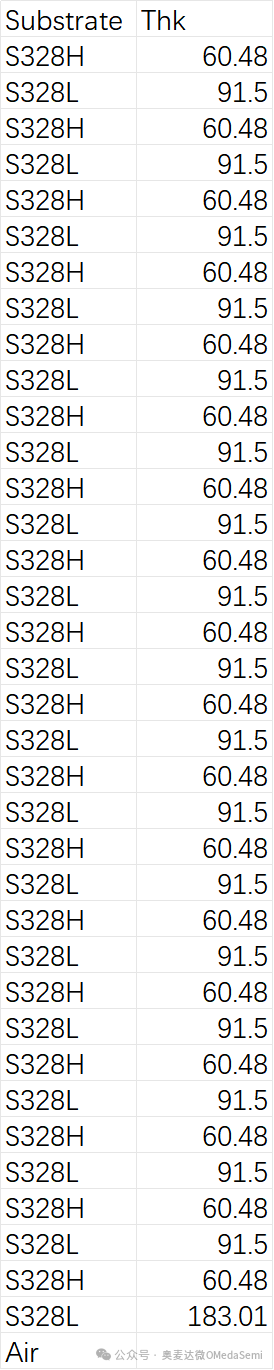
Film Stack Simulation Data:
OMeda (Shanghai Omedasemi Co.,Ltd) was founded in 2021 by 3 doctors with more than 10 years of experience in nanpfabrication. It currently has 15 employees and has rich experience in nanofabrication (coating, lithography, etching, two-photon printing, bonding) and other processes. We support nanofabrication of 4/6/8-inch wafers.
