Website:en.omedasemi.com
TEL:+8618823340140
email:jing.chen@omeda-optics.com
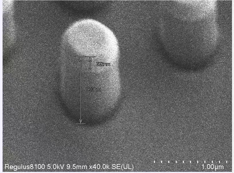
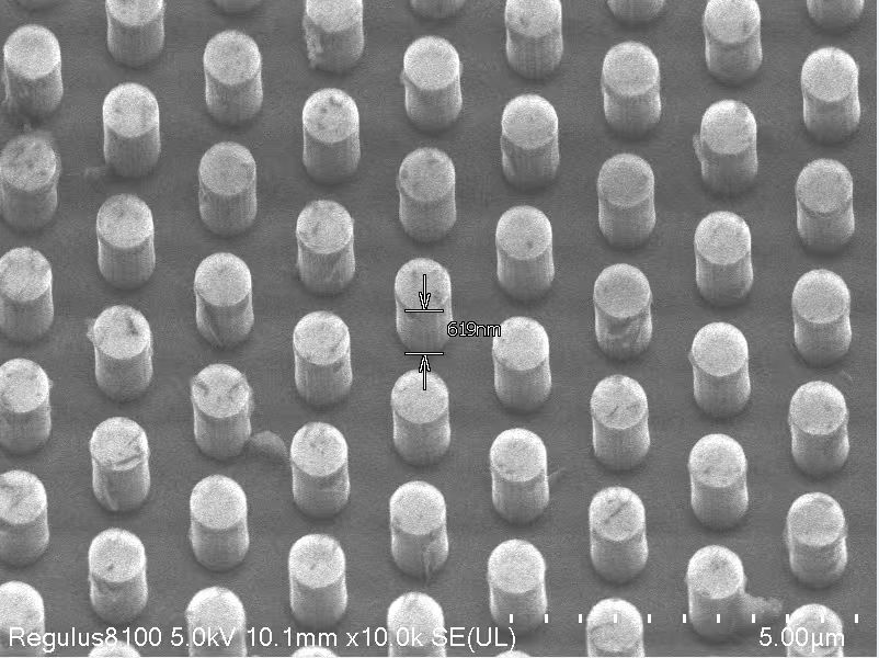
Diamond Etching Capbility
Minimum linewidth: 100nm
Etching aspect ratio: 10:1
Maximum etching depth: 2µm
Application market: Diamond photonic crystal cavity
OMeda (Shanghai Omedasemi Co.,Ltd) was founded in 2021 by 3 doctors with more than 10 years of experience in nanpfabrication. It currently has 15 employees and has rich experience in nanofabrication (coating, lithography, etching, two-photon printing, bonding) and other processes. We support nanofabrication of 4/6/8-inch wafers.